ZHCSMU8C March 2020 – July 2021 TPS54JA20
PRODUCTION DATA
- 1 特性
- 2 应用
- 3 说明
- 4 Revision History
- 5 Pin Configuration and Functions
- 6 Specifications
-
7 Detailed Description
- 7.1 Overview
- 7.2 Functional Block Diagram
- 7.3
Feature Description
- 7.3.1 Internal VCC LDO And Using External Bias On VCC Pin
- 7.3.2 Enable
- 7.3.3 Output Voltage Setting
- 7.3.4 Internal Fixed Soft Start and External Adjustable Soft Start
- 7.3.5 External REFIN For Output Voltage Tracking
- 7.3.6 Frequency and Operation Mode Selection
- 7.3.7 D-CAP3 Control
- 7.3.8 Low-side FET Zero-Crossing
- 7.3.9 Current Sense and Positive Overcurrent Protection
- 7.3.10 Low-side FET Negative Current Limit
- 7.3.11 Power Good
- 7.3.12 Overvoltage and Undervoltage Protection
- 7.3.13 Out-Of-Bounds (OOB) Operation
- 7.3.14 Output Voltage Discharge
- 7.3.15 UVLO Protection
- 7.3.16 Thermal Shutdown
- 7.4 Device Functional Modes
-
8 Application and Implementation
- 8.1 Application Information
- 8.2
Typical Application
- 8.2.1 Design Requirements
- 8.2.2
Detailed Design Procedure
- 8.2.2.1 Output Voltage Setting Point
- 8.2.2.2 Choose the Switching Frequency and the Operation Mode
- 8.2.2.3 Choose the Inductor
- 8.2.2.4 Set the Current Limit (TRIP)
- 8.2.2.5 Choose the Output Capacitor
- 8.2.2.6 Choose the Input Capacitors (CIN)
- 8.2.2.7 Soft Start Capacitor (SS/REFIN Pin)
- 8.2.2.8 EN Pin Resistor Divider
- 8.2.2.9 VCC Bypass Capacitor
- 8.2.2.10 BOOT Capacitor
- 8.2.2.11 PGOOD Pullup Resistor
- 8.2.3 Application Curves
- 9 Power Supply Recommendations
- 10Layout
- 11Device and Documentation Support
- 12Mechanical, Packaging, and Orderable Information
8.2.3 Application Curves
 Figure 8-2 Efficiency vs Output Current, VCC = 3.3V External VCC Bias
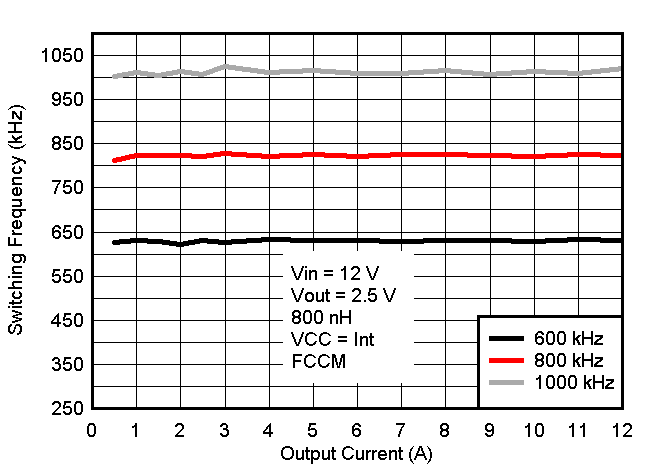 Figure 8-4 Switching Frequency vs Output Current
 Figure 8-6 Switching Frequency vs Output Voltage
 Figure 8-8 Output Voltage vs Output Current
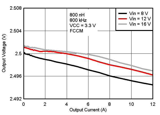 Figure 8-10 Output Voltage vs Output Current, VCC = 3.3V External Bias
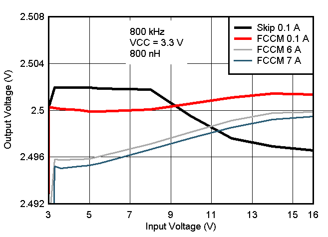 Figure 8-12 Output Voltage vs Input Voltage VCC = 3.3 V External Bias
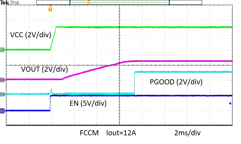 Figure 8-14 Enable Start-Up, Full Load
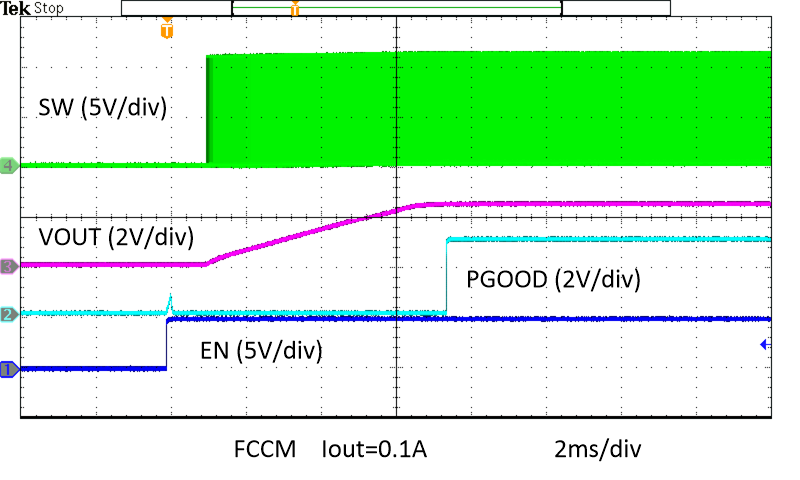 Figure 8-16 Enable to Power Up Iout = 0.1 A
 Figure 8-18 Enable Start-Up, Prebias
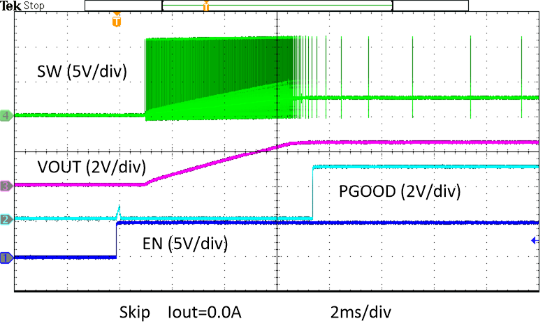 Figure 8-20 Enable Power Up, Skip
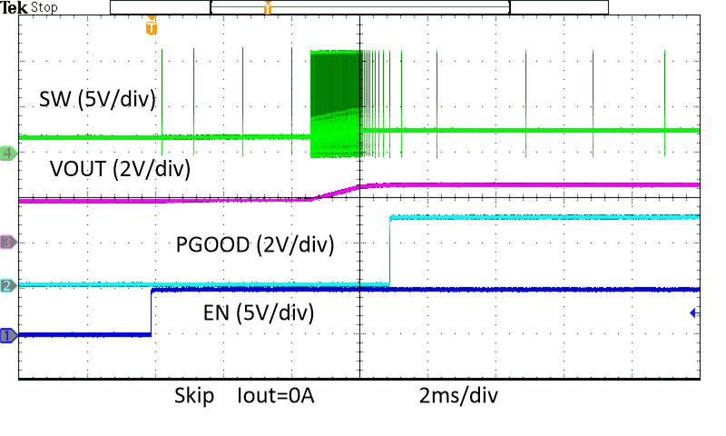 Figure 8-22 Enable Power Up into Pre-bias, Skip
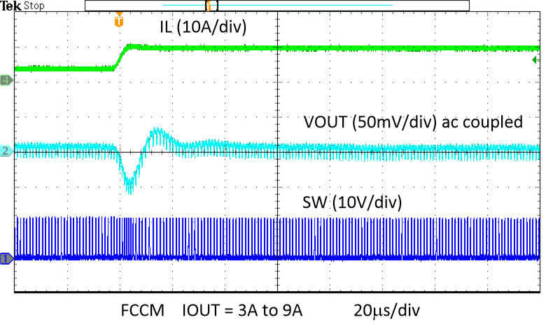 Figure 8-24 FCCM
Mode Load Transient
 Figure 8-26 Output Voltage Ripple
 Figure 8-28 Output Voltage Ripple
 Figure 8-30 Output Voltage Ripple, Skip
 Figure 8-32 Enable into Overcurrent
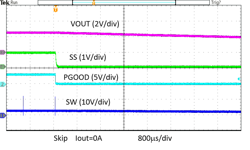 Figure 8-34 Over
Temperature Protection in Skip
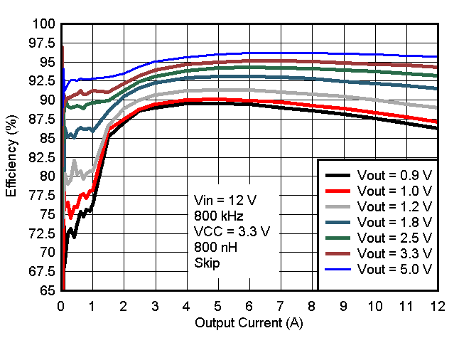 Figure 8-3 Efficiency vs Output Current, VCC = 3.3V External VCC Bias
 Figure 8-5 Switching Frequency vs Input Voltage
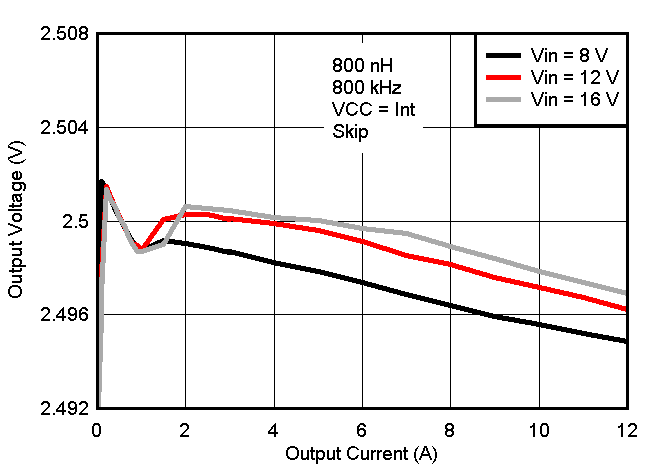 Figure 8-7 Output Voltage vs Output Current
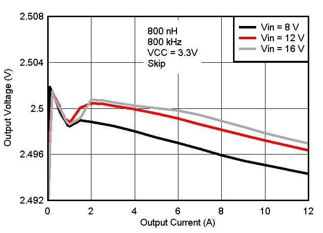 Figure 8-9 Output Voltage vs Output Current, VCC = 3.3V External Bias
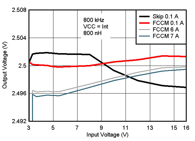 Figure 8-11 Output Voltage vs Input Voltage VCC = Int
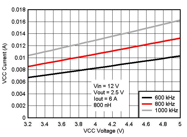 Figure 8-13 ICC
Current vs External VCC Voltage
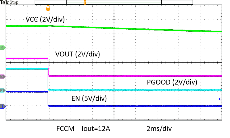 Figure 8-15 Enable Power Down Full Load
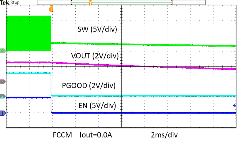 Figure 8-17 Enable to over Down Iout = 0 A
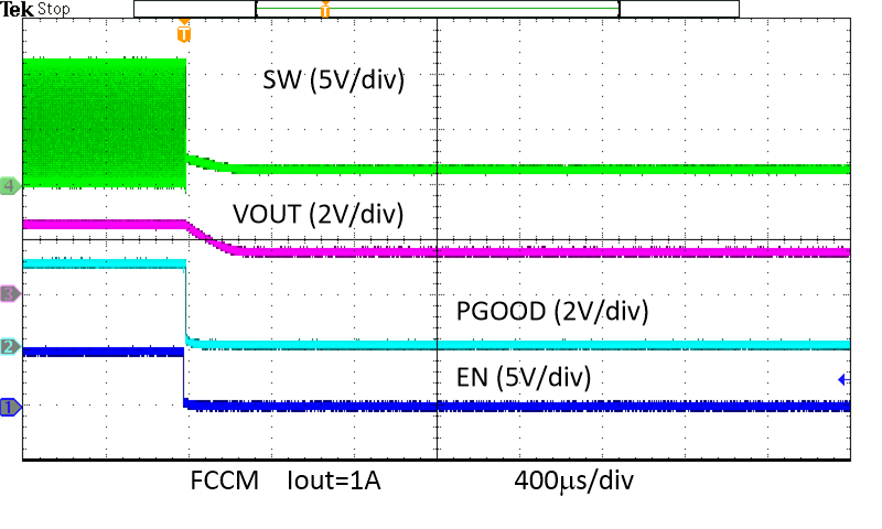 Figure 8-19 Prebias Power Up
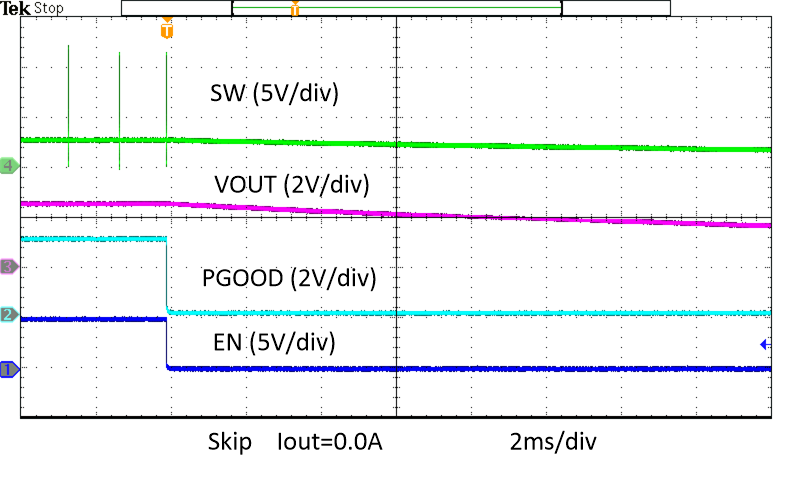 Figure 8-21 Enable Power Down, Skip
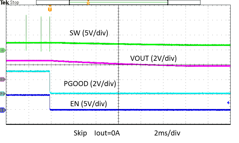 Figure 8-23 Enable Power Down with Pre-bias, Skip
 Figure 8-25 Unload Transient
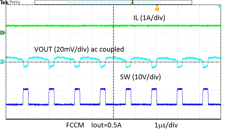 Figure 8-27 Output Voltage Ripple
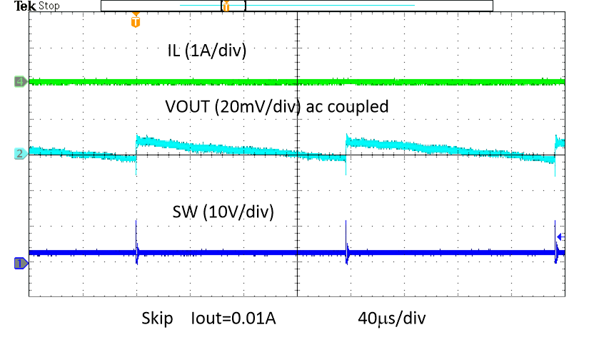 Figure 8-29 Output Voltage Ripple, Skip
 Figure 8-31 Over
Current Protection
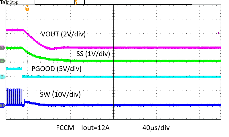 Figure 8-33 Over
Temperature Protection in FCCM
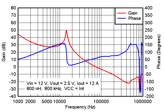 Figure 8-35 Frequency Response, 12-A
Load