ZHCSKY4B November 2018 – December 2020 TPS55288
PRODUCTION DATA
- 1 特性
- 2 应用
- 3 说明
- 4 Revision History
- 5 Pin Configuration and Functions
- 6 Specifications
-
7 Detailed Description
- 7.1 Overview
- 7.2 Functional Block Diagram
- 7.3
Feature Description
- 7.3.1 VCC Power Supply
- 7.3.2 Operation Mode Setting
- 7.3.3 Input Undervoltage Lockout
- 7.3.4 Enable and Programmable UVLO
- 7.3.5 Soft Start
- 7.3.6 Shutdown and Load Discharge
- 7.3.7 Switching Frequency
- 7.3.8 Switching Frequency Dithering
- 7.3.9 Inductor Current Limit
- 7.3.10 Internal Charge Path
- 7.3.11 Output Voltage Setting
- 7.3.12 Output Current Monitoring and Cable Voltage Droop Compensation
- 7.3.13 Integrated Gate Drivers
- 7.3.14 Output Current Limit
- 7.3.15 Overvoltage Protection
- 7.3.16 Output Short Circuit Protection
- 7.3.17 Thermal Shutdown
- 7.4 Device Functional Modes
- 7.5 I2C Serial Interface
- 7.6
Register Maps
- 7.6.1 REF Register (Address = 0h, 1h) [reset = 11010010h, 00000000h]
- 7.6.2 IOUT_LIMIT Register (Address = 2h) [reset = 11100100h]
- 7.6.3 VOUT_SR Register (Address = 3h) [reset = 00000001h]
- 7.6.4 VOUT_FS Register (Address = 4h) [reset = 00000011h]
- 7.6.5 CDC Register (Address = 5h) [reset = 11100000h]
- 7.6.6 MODE Register (Address = 6h) [reset = 00100000h]
- 7.6.7 STATUS Register (Address = 7h) [reset = 00000011h]
- 7.6.8 Register Summary
- 8 Application and Implementation
- 9 Power Supply Recommendations
- 10Layout
- 11Device and Documentation Support
- 12Mechanical, Packaging, and Orderable Information
8.2 Typical Application
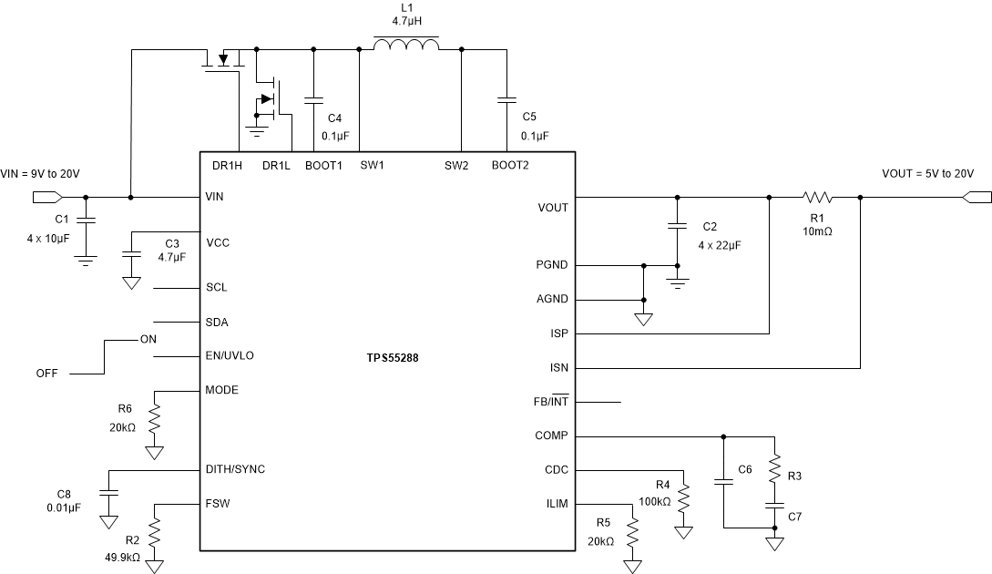
The TPS55288 provides a small size solution for USB PD power supply application with the input voltage ranging from 9 V to 20 V.
 Figure 8-1 USB PD Power Supply With 9-V to 20-V
Input Voltage