ZHCSB48B May 2013 – January 2019 TPS55330
PRODUCTION DATA.
- 1 特性
- 2 应用
- 3 说明
- 4 修订历史记录
- 5 Pin Configuration and Functions
- 6 Specifications
- 7 Detailed Description
-
8 Application and Implementation
- 8.1 Application Information
- 8.2
Typical Application
- 8.2.1 Design Requirements
- 8.2.2
Detailed Design Procedure
- 8.2.2.1 Custom Design With WEBENCH® Tools
- 8.2.2.2 Selecting the Switching Frequency (R4)
- 8.2.2.3 Determining the Duty Cycle
- 8.2.2.4 Selecting the Inductor (L1)
- 8.2.2.5 Computing the Maximum Output Current
- 8.2.2.6 Selecting the Output Capacitor (C8-C10)
- 8.2.2.7 Selecting the Input Capacitors (C2, C7)
- 8.2.2.8 Setting Output Voltage (R1, R2)
- 8.2.2.9 Setting the Soft-start Time (C7)
- 8.2.2.10 Selecting the Schottky Diode (D1)
- 8.2.2.11 Compensating the Control Loop (R3, C4, C5)
- 8.2.3 Application Curves
- 9 Power Supply Recommendations
- 10Layout
- 11器件和文档支持
- 12机械、封装和可订购信息
8.2.3 Application Curves
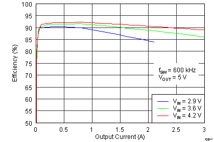 Figure 18. Efficiency vs Output Current
 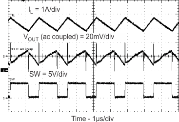 Figure 20. CCM PWM Operation
 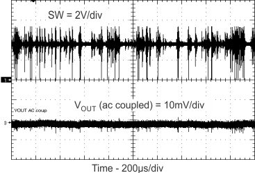 Figure 22. Pulse Skipping
 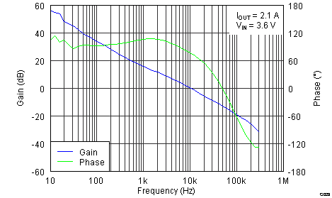 Figure 24. Closed-Loop Gain and Phase of the Boost Converter
 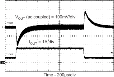 Figure 19. Load Transient Response
 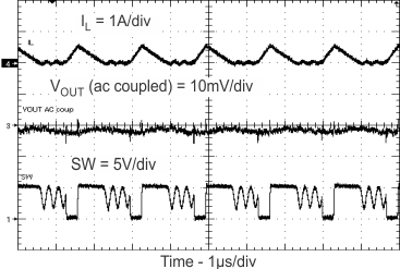 Figure 21. DCM PWM Operation
 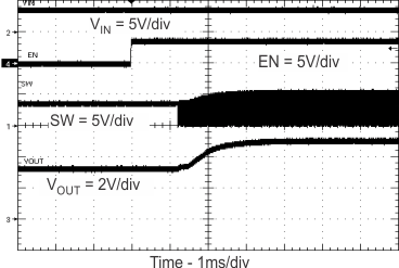 Figure 23. Start Up