ZHCSI48B September   2017  – June 2018 TPS560430

UNLESS OTHERWISE NOTED, this document contains PRODUCTION DATA.  

  1. 特性
  2. 应用
  3. 说明
    1.     Device Images
      1.      简化原理图
      2.      效率与输出电流间的关系 VOUT = 5V,1100kHz,PFM
  4. 修订历史记录
  5. Device Comparison Table
  6. Pin Configuration and Functions
    1.     Pin Functions
  7. Specifications
    1. 7.1 Absolute Maximum Ratings
    2. 7.2 ESD Ratings
    3. 7.3 Recommended Operating Conditions
    4. 7.4 Thermal Information
    5. 7.5 Electrical Characteristics
    6. 7.6 Timing Requirements
    7. 7.7 Switching Characteristics
    8. 7.8 Typical Characteristics
  8. Detailed Description
    1. 8.1 Overview
    2. 8.2 Functional Block Diagram
    3. 8.3 Feature Description
      1. 8.3.1 Fixed Frequency Peak Current Mode Control
      2. 8.3.2 Adjustable Output Voltage
      3. 8.3.3 Enable
      4. 8.3.4 Minimum ON-Time, Minimum OFF-Time and Frequency Foldback
      5. 8.3.5 Bootstrap Voltage
      6. 8.3.6 Over Current and Short Circuit Protection
      7. 8.3.7 Soft Start
      8. 8.3.8 Thermal Shutdown
    4. 8.4 Device Functional Modes
      1. 8.4.1 Shutdown Mode
      2. 8.4.2 Active Mode
      3. 8.4.3 CCM Mode
      4. 8.4.4 Light-Load Operation (PFM Version)
      5. 8.4.5 Light-Load Operation (FPWM Version)
  9. Application and Implementation
    1. 9.1 Application Information
    2. 9.2 Typical Application
      1. 9.2.1 Design Requirements
      2. 9.2.2 Detailed Design Procedure
        1. 9.2.2.1 Custom Design With WEBENCH® Tools
        2. 9.2.2.2 Output Voltage Set-Point
        3. 9.2.2.3 Switching Frequency
        4. 9.2.2.4 Inductor Selection
        5. 9.2.2.5 Output Capacitor Selection
        6. 9.2.2.6 Input Capacitor Selection
        7. 9.2.2.7 Bootstrap Capacitor
        8. 9.2.2.8 Under Voltage Lockout Set-Point
      3. 9.2.3 Application Curves
  10. 10Power Supply Recommendations
  11. 11Layout
    1. 11.1 Layout Guidelines
      1. 11.1.1 Compact Layout for EMI Reduction
      2. 11.1.2 Feedback Resistors
    2. 11.2 Layout Example
  12. 12器件和文档支持
    1. 12.1 器件支持
      1. 12.1.1 开发支持
        1. 12.1.1.1 使用 WEBENCH® 工具创建定制设计
    2. 12.2 文档支持
      1. 12.2.1 相关文档
    3. 12.3 接收文档更新通知
    4. 12.4 社区资源
    5. 12.5 商标
    6. 12.6 静电放电警告
    7. 12.7 术语表
  13. 13机械、封装和可订购信息

封装选项

请参考 PDF 数据表获取器件具体的封装图。

机械数据 (封装 | 引脚)
  • DBV|6
散热焊盘机械数据 (封装 | 引脚)
订购信息

Enable

The voltage on the EN pin controls the ON or OFF operation of TPS560430. A voltage of less than 0.95 V shuts down the device, while a voltage of more than 1.36 V is required to start the regulator. The EN pin is an input and cannot be left open or floating. The simplest way to enable the operation of the TPS560430 is to connect the EN to VIN. This allows self-start-up of the TPS560430 when VIN is within the operating range.

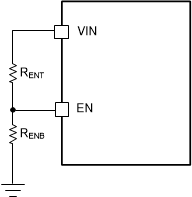
Many applications will benefit from the employment of an enable divider RENT and RENB (Figure 15) to establish a precision system UVLO level for the converter. System UVLO can be used for supplies operating from utility power as well as battery power. It can be used for sequencing, ensuring reliable operation, or supply protection, such as a battery discharge level. An external logic signal can also be used to drive EN input for system sequencing and protection. Kindly note that, the EN pin voltage should never be higher than VIN + 0.3 V. It is not recommended to apply EN voltage when VIN is 0 V.
TPS560430 slvse22-vin-uvlo-setting.gifFigure 15. System UVLO by Enable Divider