SLUSAH4D MARCH 2011 – February 2016 TPS56121
PRODUCTION DATA.
- 1 Features
- 2 Applications
- 3 Description
- 4 Revision History
- 5 Pin Configuration and Functions
- 6 Specifications
-
7 Detailed Description
- 7.1 Overview
- 7.2 Functional Block Diagram
- 7.3 Feature Description
- 7.4 Device Functional Modes
-
8 Application and Implementation
- 8.1 Application Information
- 8.2
Typical Application
- 8.2.1 Design Requirements
- 8.2.2
Detailed Design Procedure
- 8.2.2.1 Switching Frequency Selection
- 8.2.2.2 Inductor Selection (L1)
- 8.2.2.3 Output Capacitor Selection
- 8.2.2.4 Inductor Peak Current Rating
- 8.2.2.5 Input Capacitor Selection
- 8.2.2.6 Bootstrap Capacitor (C14)
- 8.2.2.7 Bootstrap Resistor (R2)
- 8.2.2.8 RC Snubber (R9 and C18)
- 8.2.2.9 VDD Bypass Capacitor (C11)
- 8.2.2.10 BP5 Bypass Capacitor (C12)
- 8.2.2.11 Soft-Start Capacitor (C13)
- 8.2.2.12 Current Limit (R1)
- 8.2.2.13 Feedback Divider (R4, R7)
- 8.2.2.14 Compensation (C15, C16, C17, R3, R6)
- 8.2.3 Application Curves
- 9 Power Supply Recommendations
- 10Layout
- 11Device and Documentation Support
- 12Mechanical, Packaging, and Orderable Information
7 Detailed Description
7.1 Overview
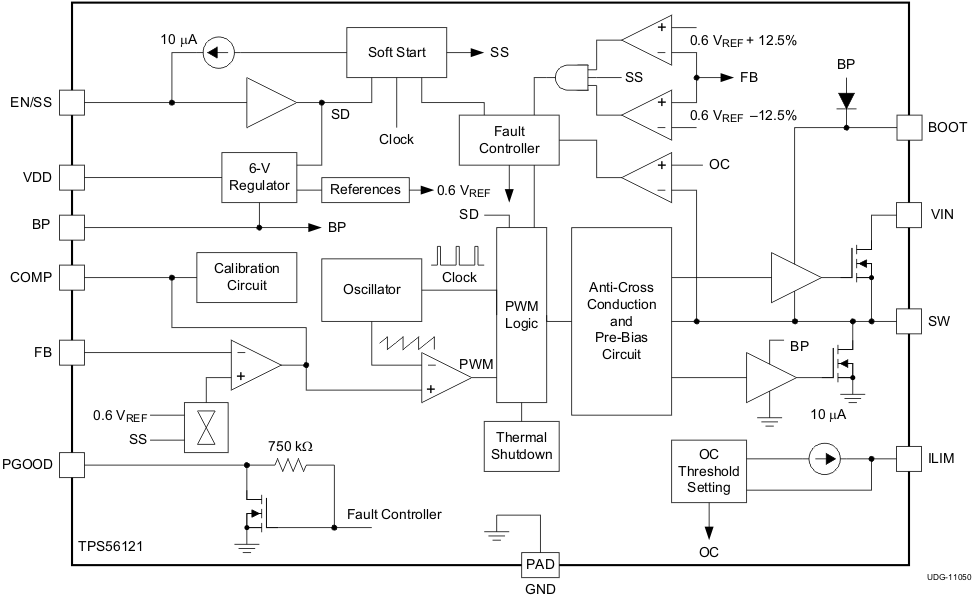
The TPS56121 is a 15-A high performance synchronous buck converter with two integrated N-channel NexFET power MOSFETs. The device implements a voltage-mode control with voltage feed-forward compensation that responds instantly to input voltage change. Pre-bias capability eliminates concerns about damaging sensitive loads.
7.2 Functional Block Diagram

7.3 Feature Description
7.3.1 Voltage Reference
The 600-mV bandgap cell is internally connected to the non-inverting input of the error amplifier. The reference voltage is trimmed with the error amplifier in a unity gain configuration to remove amplifier offset from the final regulation voltage. The 1% tolerance on the reference voltage allows the user to design a very accurate power supply.
 Figure 19. Startup Sequence and Timing
7.3.2 Enable Functionality, Startup Sequence and Timing
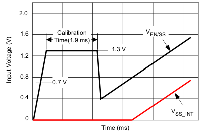
After input power is applied, an internal 40-μA current source begins to charge the soft-start capacitor connected from EN/SS to GND. When the voltage across that capacitor increases to 0.7 V, it enables the internal BP regulator followed by a calibration. Total calibration time is approximately 1.9 ms. See Figure 19. During the calibration, the device performs the following two functions.
7.3.2.1 COMP Pin Impedance Sensing
The device samples the impedance at the COMP pin and determines the appropriate operating switching frequency. If there is no resistor connected from the COMP pin to GND, the switching frequency is set to the default value of 500 kHz. If a resistor of 40.2 kΩ ± 10% is connected from the COMP pin to GND, the switching frequency is set to 300 kHz. Alternatively, if a resistor of 13.3 K ± 10% is connected from the COMP pin to GND, the switching frequency is set to 1 MHz.
After a 1.1-ms time period, the COMP pin is then brought low for 0.8 ms. This ensures that the feedback loop is preconditioned at startup and no sudden output rise occurs at the output of the converter when it is allowed to start switching.
7.3.2.2 Overcurrent Protection (OCP) Setting
The device sources 10 μA (typical) to the resistor connected from the ILIM pin to GND. The voltage developed across that resistor multiplied by a factor of 2 is then sampled and latched off internally as the OCP trip level for the low-side FET until one cycles the input or toggles the EN/SS.
The voltage at EN/SS is internally clamped to 1.3 V before and/or during calibration to minimize the discharging time once calibration is complete. The discharging current is from an internal current source of 140 μA and it pulls the voltage down to 0.4 V. It then initiates the soft-start by charging up the capacitor using an internal current source of 10 μA. The resulting voltage ramp on this pin is used as a second non-inverting input to the error amplifier after an 800 mV (typical) downward level-shift; therefore, the actual soft-start does not take place until the voltage at this pin reaches 800 mV.
If the EN/SS pin is left floating, the controller starts automatically. EN/SS must be pulled down to less than 270 mV to ensure that the chip is in shutdown mode.
7.3.3 Soft-Start Time
The soft-start time of the TPS56121 is user programmable by selecting a single capacitor. The EN/SS pin sources 10 μA to charge this capacitor. The actual output ramp-up time is the amount of time that it takes for the 10 μA to charge the capacitor through a 600 mV range. There is some initial lag due to calibration and an offset (800 mV) from the actual EN/SS pin voltage to the voltage applied to the error amplifier.
The soft-start is accomplished in a closed-loop, meaning that the error amplifier controls the output voltage at all times during the soft-start period and the feedback loop is never open as occurs in duty cycle limit soft-start schemes. The error amplifier has two non-inverting inputs, one connected to the 600-mV reference voltage, and the other connected to the offset EN/SS pin voltage. The lower of these two voltages is what the error amplifier controls the FB pin to. As the voltage on the EN/SS pin ramps up past approximately 1.4 V (800 mV offset voltage plus the 600 mV reference voltage), the 600-mV reference voltage becomes the dominant input and the converter has reached its final regulation voltage.
The capacitance required for a given soft-start ramp time for the output voltage is calculated in Equation 1.

where
- CSS is the required capacitance on the EN/SS pin (nF)
- ISS is the soft-start source current (10 μA)
- VFB is the feedback reference voltage (0.6 V)
- tSS is the desired soft-start ramp time (ms)
7.3.4 Oscillator
The oscillator frequency is internally fixed at 500 KHz if there is no resistor connected from COMP pin to GND. Optionally, a 40.2-kΩ resistor from the COMP pin to GND sets the frequency to 300 KHz. Alternatively, a 13.3-kΩ resistor from COMP pin GND sets the frequency to 1 MHz.
7.3.5 Overcurrent Protection (OCP)
Programmable OCP level at ILIM is from 6 mV to 50 mV. With a scale factor of 2, the actual OC trip point across the low-side FET is in the range of 12 mV to 100 mV.
If the voltage drop across ROCSET reaches 300 mV during calibration (No ROCSET resistor included), it disables OC protection. Once disabled, there is no low-side or high-side current sensing.
OCP level for the high-side FET is fixed at 34 A (typical). The high-side OCP provides pulse-by-pulse current limiting.
OCP sensing for the low-side FET is a true inductor valley current detection, using sample and hold. Equation 2 can be used to calculate ROCSET. Since the TPS56121 is designed for 15-A full-Load current and not intentionally designed for an OCP level below 10 A, use an ROCSET value above 1 kΩ to get an accurate OCP tripping point.

where
- IP-P is the peak-to-peak inductor current (A)
- IOUT(max) is the trip point for OCP (A)
- ROCSET is the resistor used for setting the OCP level (Ω)
An overcurrent (OC) condition is detected by sensing voltage drop across the low-side FET and across the high-side FET. If the voltage drop across either FET exceeds OC threshold, a count increments one count. If no OC condition is detected on either FET, the fault counter decrements by one counter. If three OC pulses are summed, a fault condition is declared which cycles the soft-start function in a hiccup mode. Hiccup mode is defined as four dummy soft-start timeouts followed by a real one if overcurrent condition is encountered during normal operation; or five dummy soft-start timeouts followed by a real one if overcurrent condition occurs from the beginning during start. This cycle continues indefinitely until the fault condition is removed.
7.3.6 Switching Node (SW)
The SW pin connects to the switching node of the power conversion stage. It acts as the return path for the high-side gate driver. When configured as a synchronous buck stage, the voltage swing on SW normally traverses from below ground to well above the input voltage. Parasitic inductance in the high-side FET and the output capacitance (COSS) of both power FETs form a resonant circuit that can produce high frequency ( > 100 MHz) ringing on this node. The voltage peak of this ringing, if not controlled, can be significantly higher than the input voltage. Ensure that the peak ringing amplitude does not exceed the absolute maximum rating limit for the pin.
In many cases, a series resistor and capacitor snubber network connected from the switching node to PGND can be helpful in damping the ringing and decreasing the peak amplitude. Provide provisions for snubber network components in the layout of the printed circuit board. If testing reveals that the ringing amplitude at the SW pin exceeds the limit, then include snubber components.
Placing a BOOT resistor with a value between 5 Ω and 15 Ω in series with the BOOT capacitor slows down the turn-on of the high-side FET and can help to reduce the peak ringing at the switching node as well.
7.3.7 Input Undervoltage Lockout (UVLO)
The TPS56121 has fixed input UVLO. In order for the device to turn on, the following conditions must be met:
- the EN/SS pin voltage must be greater than VIH
- the input voltage must exceed UVLO on voltage VUVLO
The UVLO has a minimum of 500 mV hysteresis built-in.
7.3.8 Pre-Bias Startup
The TPS56121 contains a unique circuit to prevent current from being pulled from the output during startup in the condition the output is pre-biased. There are no PWM pulses until the internal soft-start voltage rises above the error amplifier input (FB pin), if the output is pre-biased. Once the soft-start voltage exceeds the error amplifier input, the controller slowly initiates synchronous rectification by starting the synchronous rectifier with a narrow on time. It then increments the on-time on a cycle-by-cycle basis until it coincides with the time dictated by (1-D), where D is the duty cycle of the converter.
This approach prevents the sinking of current from a pre-biased output, and ensures the output voltage startup and ramp to regulation is smooth and controlled.
7.3.9 Power Good
The TPS56121 provides an indication that output is good for the converter. This is an open drain signal and pulls low when any condition exists that would indicate that the output of the supply might be out of regulation. These conditions include:
- VFB is more than ±12.5% from nominal
- soft-start is active
- a short circuit condition has been detected
NOTE
When there is no power to the device, PGOOD is not able to pull close to GND if an auxiliary supply is used for the power good indication. In this case, a built in resistor connected from drain to gate on the PGOOD pull down device makes the PGOOD pin look approximately like a diode to GND.
7.4 Device Functional Modes
The TPS56121 devices operate in continuous conduction mode (CCM) at a fixed frequency, regardless of the output current. For the first 128 switching cycles, the low-side MOSFET on-time is slowly increased to prevent excessive current sinking in the event the device is started with a prebiased output. Following the first 128 switching cycles, the low-side MOSFET and the high-side MOSFET on-times are fully complementary.