SLUSAH4D MARCH 2011 – February 2016 TPS56121
PRODUCTION DATA.
- 1 Features
- 2 Applications
- 3 Description
- 4 Revision History
- 5 Pin Configuration and Functions
- 6 Specifications
-
7 Detailed Description
- 7.1 Overview
- 7.2 Functional Block Diagram
- 7.3 Feature Description
- 7.4 Device Functional Modes
-
8 Application and Implementation
- 8.1 Application Information
- 8.2
Typical Application
- 8.2.1 Design Requirements
- 8.2.2
Detailed Design Procedure
- 8.2.2.1 Switching Frequency Selection
- 8.2.2.2 Inductor Selection (L1)
- 8.2.2.3 Output Capacitor Selection
- 8.2.2.4 Inductor Peak Current Rating
- 8.2.2.5 Input Capacitor Selection
- 8.2.2.6 Bootstrap Capacitor (C14)
- 8.2.2.7 Bootstrap Resistor (R2)
- 8.2.2.8 RC Snubber (R9 and C18)
- 8.2.2.9 VDD Bypass Capacitor (C11)
- 8.2.2.10 BP5 Bypass Capacitor (C12)
- 8.2.2.11 Soft-Start Capacitor (C13)
- 8.2.2.12 Current Limit (R1)
- 8.2.2.13 Feedback Divider (R4, R7)
- 8.2.2.14 Compensation (C15, C16, C17, R3, R6)
- 8.2.3 Application Curves
- 9 Power Supply Recommendations
- 10Layout
- 11Device and Documentation Support
- 12Mechanical, Packaging, and Orderable Information
10 Layout
10.1 Layout Guidelines
- Place input capacitors next to the VIN pin and on the same side as the device. Use wide and short traces or copper planes for the connection from the VIN pin to the input capacitor and from the input capacitor to the power pad of the device.
- Place the BP decoupling capacitor close to the BP pin and on the same side as the device in order to avoid the use of vias. Use wide and short traces for the connection from the BP pin to the capacitor and from the capacitor to the power pad. If vias are not evitable, use at least three vias to reduce the parasitic inductance.
- Include a Kelvin VDD connection, or separate from VIN connection (bypass input capacitors); add a placeholder for a filter resistor between the VDD pin and the input bus. Place the VDD decoupling capacitor near the VDD pin and on the same side as the device to avoid the use of vias. Use wide and short traces for the connection from the VDD pin to the capacitor and from the capacitor to the power pad of the device. If vias are not avoidable, use at least three vias to reduce the parasitic inductance.
- Maintain the FB trace away from BOOT and SW traces.
- Minimize the area of switch node.
- Use a single ground.Do not use separate signal and power ground.
- Use 3 × 7 thermal vias as suggested in Land Pattern Data in Mechanical, Packaging, and Orderable Information.
10.2 Layout Example
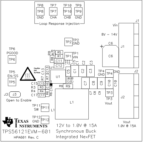
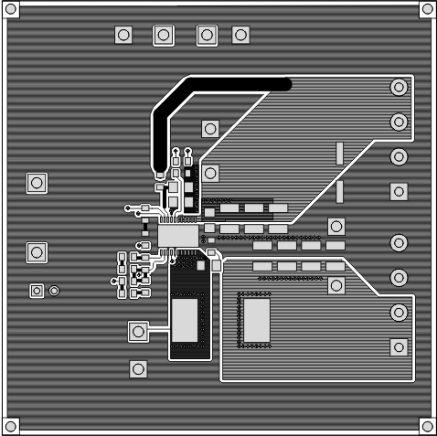
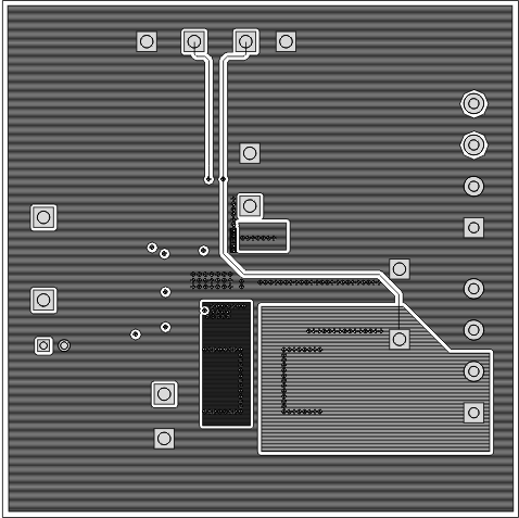
The TPS56121EVM-601 layout is shown in Figure 24 through Figure 29 for reference.
 Figure 24. TPS56121EVM-601 Top Assembly Drawing (Top view)
 Figure 26. TPS56121EVM-601 Top Copper (Top View)
 Figure 28. TPS56121EVM-601 Internal 2 (Top View)
 Figure 25. TPS56121EVM-601 Bottom Assembly Drawing (Bottom view)
 Figure 27. TPS56121EVM-601 Internal 1 (Top View)
 Figure 29. TPS56121EVM-601 Bottom Copper (Top View)