ZHCS124C MARCH 2011 – January 2015 TPS56221
PRODUCTION DATA.
- 1 特性
- 2 应用范围
- 3 说明
- 4 修订历史记录
- 5 Pin Configuration and Functions
- 6 Specifications
-
7 Detailed Description
- 7.1 Overview
- 7.2 Functional Block Diagram
- 7.3 Feature Description
- 7.4 Device Functional Modes
-
8 Application and Implementation
- 8.1 Application Information
- 8.2
Typical Application
- 8.2.1 Design Requirements
- 8.2.2
Detailed Design Procedure
- 8.2.2.1 Switching Frequency Selection
- 8.2.2.2 Inductor Selection
- 8.2.2.3 Output Capacitor Selection
- 8.2.2.4 Inductor Peak Current Rating
- 8.2.2.5 Input Capacitor Selection
- 8.2.2.6 Boot-Strap Capacitor (C14)
- 8.2.2.7 Boot-Strap Resistor (R2)
- 8.2.2.8 VDD Bypass Capacitor (C11)
- 8.2.2.9 BP5 Bypass Capacitor (C12)
- 8.2.2.10 Soft-Start Capacitor (C13)
- 8.2.2.11 Current Limit (R1)
- 8.2.2.12 Feedback Divider (R4, R7)
- 8.2.2.13 Compensation (C15, C16, C17, R3, R6)
- 8.2.3 Application Curves
- 9 Power Supply Recommendations
- 10Layout
- 11器件和文档支持
- 12机械、封装和可订购信息
封装选项
请参考 PDF 数据表获取器件具体的封装图。
机械数据 (封装 | 引脚)
- DQP|22
散热焊盘机械数据 (封装 | 引脚)
- DQP|22
订购信息
10 Layout
10.1 Layout Guidelines
- Place input capacitors next to the VIN pin and on the same side as the device. Use wide and short traces or copper planes for the connection from the VIN pin to the input capacitor and from the input capacitor to the power pad of the device.
- Place the BP decoupling capacitor close to the BP pin and on the same side as the device in order to avoid the use of vias. Use wide and short traces for the connection from the BP pin to the capacitor and from the capacitor to the power pad. If vias are not evitable, use at least three vias to reduce the parasitic inductance.
- Include a Kelvin VDD connection, or separate from VIN connection (bypass input capacitors); add a placeholder for a filter resistor between the VDD pin and the input bus. Place the VDD decoupling capacitor near the VDD pin and on the same side as the device to avoid the use of vias. Use wide and short traces for the connection from the VDD pin to the capacitor and from the capacitor to the power pad of the device. If vias are not avoidable, use at least three vias to reduce the parasitic inductance.
- Maintain the FB trace away from BOOT and SW traces.
- Minimize the area of switch node.
- Use a single ground. Do not use separate signal and power ground.
- Use 3 × 7 thermal vias as suggested in Land Pattern Data in 机械、封装和可订购信息.
10.2 Layout Example
The TPS56221EVM layout is shown in Figure 25 through Figure 30 for reference.
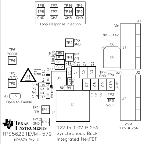 Figure 25. TPS56221EVM Top Assembly Drawing (Top view)
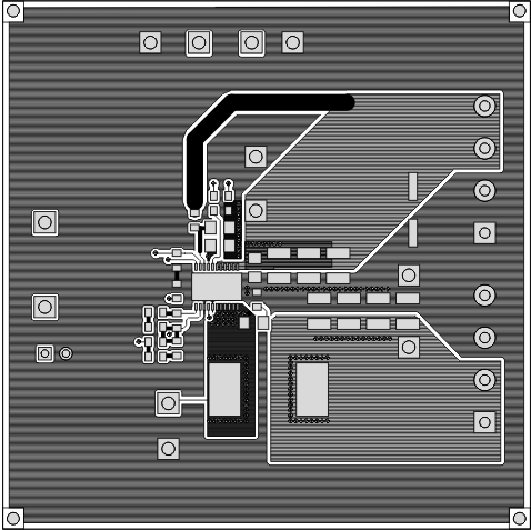 Figure 27. TPS56221EVM Top Copper (Top View)
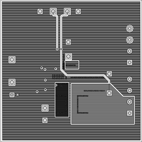 Figure 29. TPS56221EVM Internal 2 (Top View)
 Figure 26. TPS56221EVM Bottom Assembly Drawing (Bottom view)
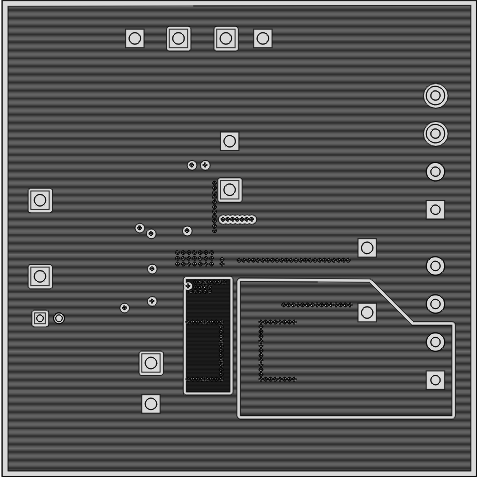 Figure 28. TPS56221EVM Internal 1 (Top View)
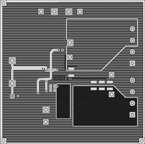 Figure 30. TPS56221EVM Bottom Copper (Top View)