ZHCS124C MARCH 2011 – January 2015 TPS56221
PRODUCTION DATA.
- 1 特性
- 2 应用范围
- 3 说明
- 4 修订历史记录
- 5 Pin Configuration and Functions
- 6 Specifications
-
7 Detailed Description
- 7.1 Overview
- 7.2 Functional Block Diagram
- 7.3 Feature Description
- 7.4 Device Functional Modes
-
8 Application and Implementation
- 8.1 Application Information
- 8.2
Typical Application
- 8.2.1 Design Requirements
- 8.2.2
Detailed Design Procedure
- 8.2.2.1 Switching Frequency Selection
- 8.2.2.2 Inductor Selection
- 8.2.2.3 Output Capacitor Selection
- 8.2.2.4 Inductor Peak Current Rating
- 8.2.2.5 Input Capacitor Selection
- 8.2.2.6 Boot-Strap Capacitor (C14)
- 8.2.2.7 Boot-Strap Resistor (R2)
- 8.2.2.8 VDD Bypass Capacitor (C11)
- 8.2.2.9 BP5 Bypass Capacitor (C12)
- 8.2.2.10 Soft-Start Capacitor (C13)
- 8.2.2.11 Current Limit (R1)
- 8.2.2.12 Feedback Divider (R4, R7)
- 8.2.2.13 Compensation (C15, C16, C17, R3, R6)
- 8.2.3 Application Curves
- 9 Power Supply Recommendations
- 10Layout
- 11器件和文档支持
- 12机械、封装和可订购信息
封装选项
请参考 PDF 数据表获取器件具体的封装图。
机械数据 (封装 | 引脚)
- DQP|22
散热焊盘机械数据 (封装 | 引脚)
- DQP|22
订购信息
6 Specifications
6.1 Absolute Maximum Ratings
over operating free-air temperature range (unless otherwise noted) (1)| MIN | MAX | UNIT | ||
|---|---|---|---|---|
| Voltage | VDD, VIN | –0.3 | 16.5 | V |
| SW | –3 | 25 | ||
| SW (< 100 ns pulse width, 10 µJ) | –5 | |||
| BOOT | –0.3 | 30 | ||
| BOOT-SW (differential from BOOT to SW) | –0.3 | 7 | ||
| COMP, PGOOD, FB, BP, EN/SS, ILIM | –0.3 | 7 | ||
| Junction Temperature, TJ | –40 | 150 | °C | |
| Storage temperature, Tstg | –55 | 150 | °C | |
(1) Stresses beyond those listed under Absolute Maximum Ratings may cause permanent damage to the device. These are stress ratings only and functional operation of the device at these or any other condition beyond those included under Recommended Operating Conditions is not implied. Exposure to absolute-maximum-rated conditions for extended periods of time may affect device reliability.
6.2 ESD Ratings
| VALUE | UNIT | |||
|---|---|---|---|---|
| V(ESD) | Electrostatic discharge | Human body model (HBM), per ANSI/ESDA/JEDEC JS-001(1) | ±2000 | V |
| Charged-device model (CDM), per JEDEC specification JESD22-C101(2) | ±1500 | |||
(1) JEDEC document JEP155 states that 500-V HBM allows safe manufacturing with a standard ESD control process.
(2) JEDEC document JEP157 states that 250-V CDM allows safe manufacturing with a standard ESD control process.
6.3 Recommended Operating Conditions
over operating free-air temperature range (unless otherwise noted)| MIN | NOM | MAX | UNIT | ||
|---|---|---|---|---|---|
| VDD | VIN Input voltage | 4.5 | 14 | V | |
| TJ | Operating junction temperature | –40 | 125 | °C |
6.4 Thermal Information
| THERMAL METRIC(1) | TPS56221 | UNIT | |
|---|---|---|---|
| PQFN | |||
| 22 PINS | |||
| RθJA | Junction-to-ambient thermal resistance | 34.6 | °C/W |
| RθJC(top) | Junction-to-case (top) thermal resistance | 22.9 | |
| ψJT | Junction-to-top characterization parameter | 0.6 | |
| ψJB | Junction-to-board characterization parameter | 5.0 | |
| RθJC(bot) | Junction-to-case (bottom) thermal resistance | 0.3 | |
(1) For more information about traditional and new thermal metrics, see the IC Package Thermal Metrics application report, SPRA953.
6.5 Electrical Characteristics
–40°C ≤ TJ ≤ 125°C, VVDD = 12 V, all parameters at zero power dissipation (unless otherwise noted)| PARAMETER | TEST CONDITIONS | MIN | TYP | MAX | UNIT | ||
|---|---|---|---|---|---|---|---|
| VOLTAGE REFERENCE | |||||||
| VFB | FB input voltage | TJ = 25°C, 4.5 V ≤ VVDD ≤ 14 V | 597 | 600 | 603 | mV | |
| –40°C ≤ TJ ≤ 125°C, 4.5 V ≤ VVDD ≤ 14 V |
594 | 600 | 606 | ||||
| INPUT SUPPLY | |||||||
| VVDD | Input supply voltage range | 4.5 | 14 | V | |||
| IVDDSD | Shutdown supply current | VEN/SS = 0.2 V | 80 | 120 | µA | ||
| IVDDQ | Quiescent, nonswitching | Let EN/SS float, VFB = 1 V | 2.5 | 5.0 | mA | ||
| VUVLO | UVLO ON Voltage | 4.0 | 4.3 | V | |||
| VUVLO(HYS) | UVLO hysteresis | 500 | 700 | mV | |||
| ENABLE/SOFT-START | |||||||
| VIH | High-level input voltage, EN/SS | 0.55 | 0.70 | 1.00 | V | ||
| VIL | Low-level input voltage, EN/SS | 0.27 | 0.30 | 0.33 | V | ||
| ISS | Soft-start source current | 8 | 10 | 12 | µA | ||
| VSS | Soft-start voltage level – start of ramp | 0.4 | 0.8 | 1.3 | V | ||
| BP REGULATOR | |||||||
| VBP | Output voltage | IBP = 10 mA | 6.2 | 6.5 | 6.8 | V | |
| VDO | Regulator dropout voltage, VVDD – VBP | IBP = 25 mA, VVDD = 4.5 V | 70 | 125 | mV | ||
| OSCILLATOR | |||||||
| fSW | Switching frequency | RCOMP = 40.2 kΩ, 4.5 V ≤ VVDD ≤ 14 V |
270 | 300 | 330 | kHz | |
| RCOMP = open, 4.5 V ≤ VVDD ≤ 14 V |
450 | 500 | 550 | kHz | |||
| RCOMP = 13.3 kΩ, 4.5 V ≤ VVDD ≤ 14 V |
0.8 | 0.95 | 1.1 | MHz | |||
| VRAMP(1) | Ramp amplitude | VVDD/6.6 | VVDD/6 | VVDD/5.4 | V | ||
| PWM | |||||||
| DMAX(1) | Maximum duty cycle | fsw = 300 kHz, VFB = 0 V, 4.5 V ≤ VVDD ≤ 14 V |
93% | ||||
| fsw = 500 kHz, VFB = 0 V, 4.5 V ≤ VVDD ≤ 14 V |
90% | ||||||
| fsw = 1 MHz, VFB = 0 V, 4.5 V ≤ VVDD ≤ 14 V |
85% | ||||||
| tON(min)(1) | Minimum controllable pulse width | 100 | ns | ||||
| ERROR AMPLIFIER | |||||||
| GBWP (1) | Gain bandwidth product | 10 | 24 | MHz | |||
| AOL (1) | Open loop gain | 60 | dB | ||||
| IIB | Input bias current (current out of FB pin) | VFB = 0.6 V | 75 | nA | |||
| IEAOP | Output source current | VFB = 0 V | 1.5 | mA | |||
| IEAOM | Output sink current | VFB = 1 V | 1.5 | mA | |||
| POWER GOOD | |||||||
| VOV | Feedback upper voltage limit for PGOOD | 655 | 675 | 700 | mV | ||
| VUV | Feedback lower voltage limit for PGOOD | 500 | 525 | 550 | mV | ||
| VPGD-HYST | PGOOD hysteresis voltage at FB | 30 | 45 | mV | |||
| RPGD | PGOOD pull down resistance | VFB = 0 V, IFB = 5 mA | 30 | 70 | Ω | ||
| IPGDLK | PGOOD leakage current | 550 mV < VFB < 655 mV, VPGOOD = 5 V |
10 | 20 | µA | ||
| OUTPUT STAGE | |||||||
| RHI | High-side device resistance | TJ = 25°C, (VBOOT– VSW) = 5.5 V | 4.5 | 6.5 | mΩ | ||
| RLO | Low side device resistance | TJ = 25°C | 1.9 | 2.7 | mΩ | ||
| OVERCURRENT PROTECTION (OCP) | |||||||
| tPSSC(min)(1) | Minimum pulse time during short circuit | 250 | ns | ||||
| tBLNKH(1) | Switch leading-edge blanking pulse time (high-side detection) | 150 | |||||
| IOCH | OC threshold for high-side FET | TJ = 25°C, (VBOOT– VSW) = 5.5 V | 45 | 54 | 65 | A | |
| IILIM | ILIM current source | TJ = 25°C | 10.0 | µA | |||
| VOCLPRO(1) | Programmable OC range for low side FET | TJ = 25°C | 12 | 100 | mV | ||
| tOFF | OC retry cycles on EN/SS pin | 4 | Cycle | ||||
| BOOT DIODE | |||||||
| VDFWD | Bootstrap diode forward voltage | IBOOT = 5 mA | 0.8 | V | |||
| THERMAL SHUTDOWN | |||||||
| TJSD(1) | Junction shutdown temperature | 145 | ºC | ||||
| TJSDH(1) | Hysteresis | 20 | ºC | ||||
(1) Ensured by design. Not production tested
6.6 Typical Characteristics
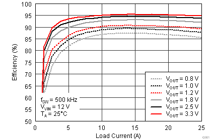
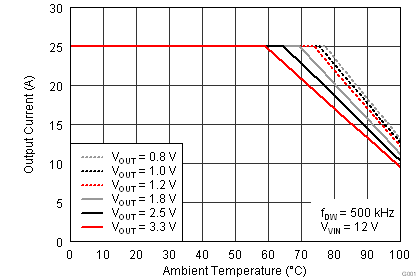
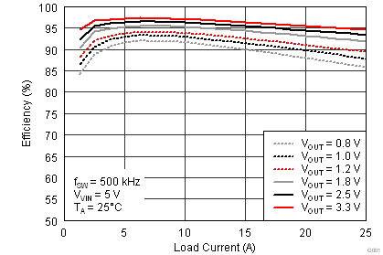
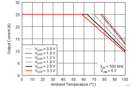
Figure 13 to Figure 18 are measured on a 2.5 inch × 2.5 inch, 0.062 inch thick FR4 board with 4 layers and 2-oz. copper, a 0.32-µH output inductor and a DCR of 0.32 mΩ.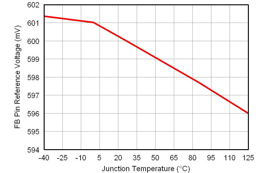 Figure 1. Reference Voltage vs. Junction Temperature
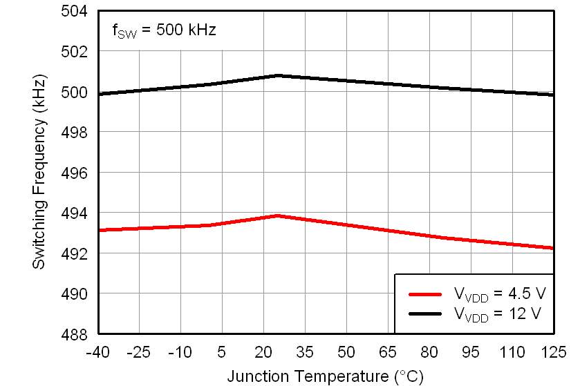 Figure 3. Switching Frequency vs. Junction Temperature (500 kHz)
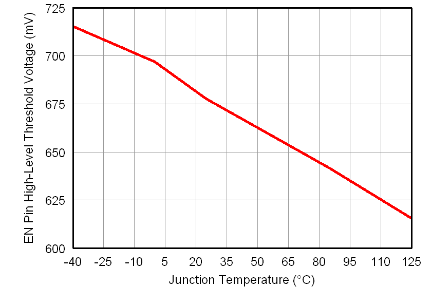 Figure 5. EN Pin High-Level Threshold Voltage vs. Junction Temperature
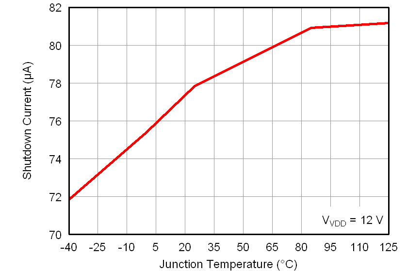 Figure 7. Shutdown Current vs. Junction Temperature
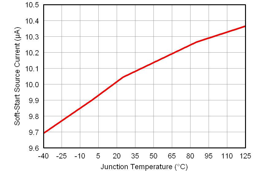 Figure 9. Soft-Start Source vs. Junction Temperature
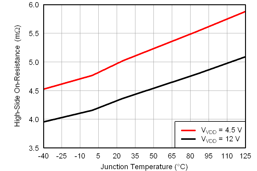 Figure 11. High-Side On Resistance vs. Junction Temperature
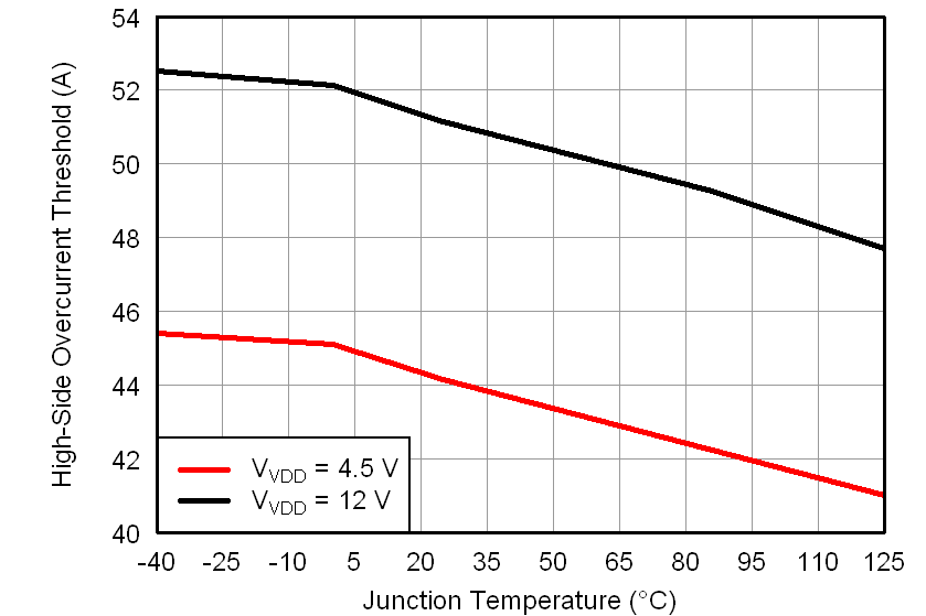 Figure 13. High-Side Overcurrent Threshold vs. Junction Temperature
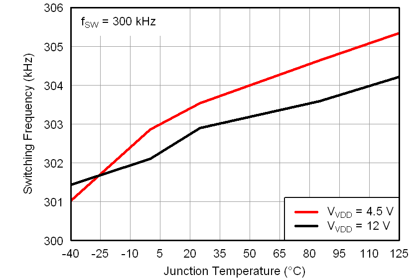 Figure 2. Switching Frequency vs. Junction Temperature (300 kHz)
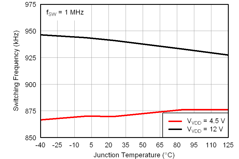 Figure 4. Switching Frequency vs. Junction Temperature (1 MHz)
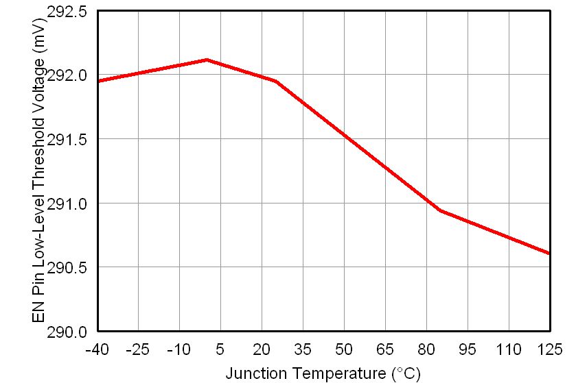 Figure 6. EN Pin Low-Level Threshold Voltage vs. Junction Temperature
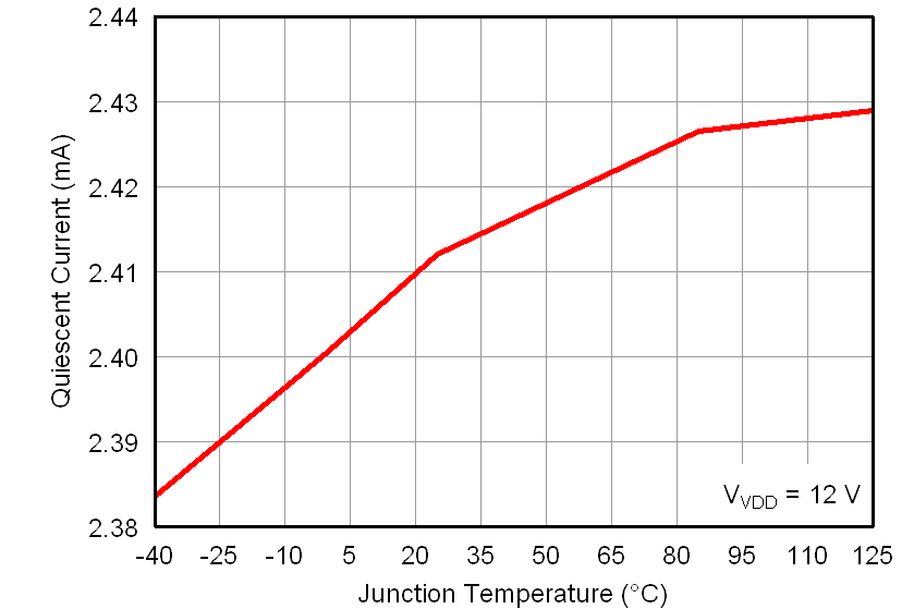 Figure 8. Quiescent Current vs. Junction Temperature
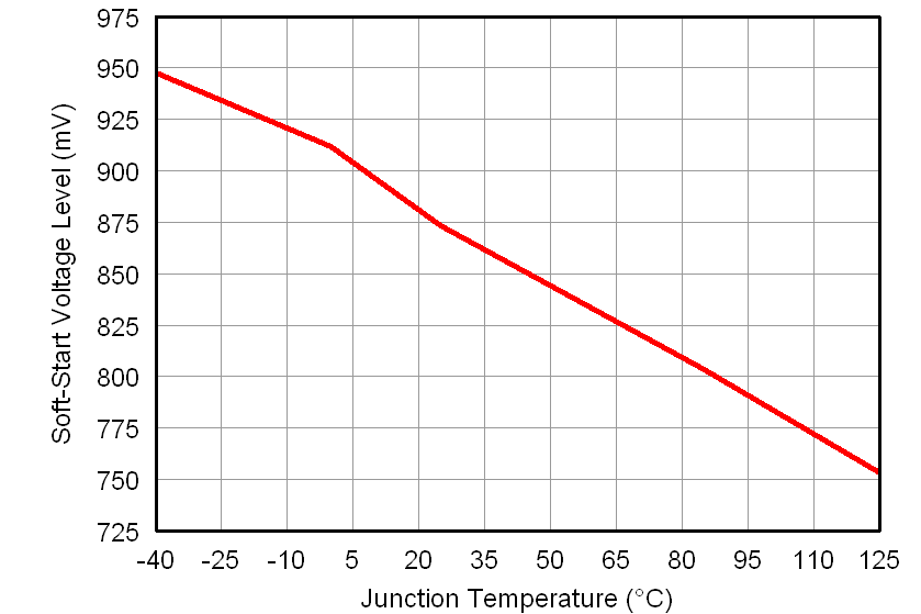 Figure 10. Soft-Start Voltage Level vs. Junction Temperature
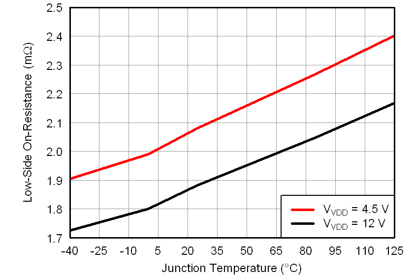 Figure 12. Low-Side On Resistance vs. Junction Temperature
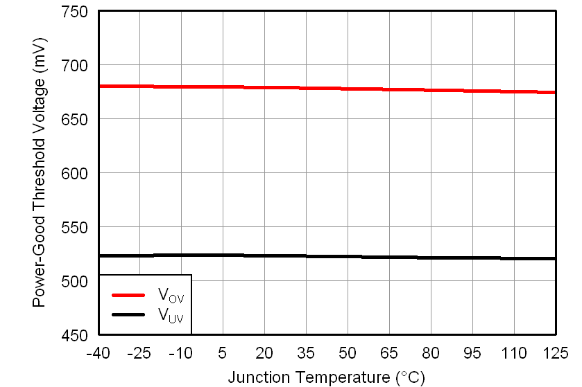 Figure 14. Power Good Threshold Voltage vs. Junction Temperature
