ZHCSCT6A September 2014 – November 2016 TPS562209 , TPS563209
PRODUCTION DATA.
- 1 特性
- 2 应用
- 3 说明
- 4 修订历史记录
- 5 Pin Configuration and Functions
- 6 Specifications
- 7 Detailed Description
- 8 Application and Implementation
- 9 Power Supply Recommendations
- 10Layout
- 11器件和文档支持
- 12机械、封装和可订购信息
7 Detailed Description
7.1 Overview
The TPS562209 and TPS563209 are 2-A and 3-A synchronous step-down converters, respectively. The proprietary D-CAP2™ mode control supports low ESR output capacitors such as specialty polymer capacitors and multi-layer ceramic capacitors without complex external compensation circuits. The fast transient response of D-CAP2™ mode control can reduce the output capacitance required to meet a specific level of performance.
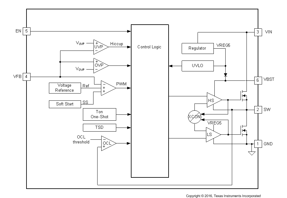
7.2 Functional Block Diagram
 Figure 19. TPS56x209
7.3 Feature Description
7.3.1 The Adaptive On-Time Control and PWM Operation
The main control loop of the TPS56x209 are adaptive on-time pulse width modulation (PWM) controller that supports a proprietary D-CAP2™ mode control. The D-CAP2™ mode control combines adaptive on-time control with an internal compensation circuit for pseudo-fixed frequency and low external component count configuration with both low ESR and ceramic output capacitors. It is stable even with virtually no ripple at the output.
At the beginning of each cycle, the high-side MOSFET is turned on. This MOSFET is turned off after internal one shot timer expires. This one shot duration is set inversely proportional to the converter input voltage, VIN, and proportional to the output voltage, VO, to maintain a pseudo-fixed frequency over the input voltage range, hence it is called adaptive on-time control. The one-shot timer is reset and the high-side MOSFET is turned on again when the feedback voltage falls below the reference voltage. An internal ramp is added to reference voltage to simulate output ripple, eliminating the need for ESR induced output ripple from D-CAP2™ mode control.
7.3.2 Soft Start and Pre-Biased Soft Start
The TPS562209 and TPS563209 have an internal 1.0ms soft-start. When the EN pin becomes high, the internal soft-start function begins ramping up the reference voltage to the PWM comparator.
If the output capacitor is pre-biased at startup, the devices initiate switching and start ramping up only after the internal reference voltage becomes greater than the feedback voltage VFB. This scheme ensures that the converters ramp up smoothly into regulation point.
7.3.3 Current Protection
The output over-current limit (OCL) is implemented using a cycle-by-cycle valley detect control circuit. The switch current is monitored during the OFF state by measuring the low-side FET drain to source voltage. This voltage is proportional to the switch current. To improve accuracy, the voltage sensing is temperature compensated. During the on time of the high-side FET switch, the switch current increases at a linear rate determined by Vin, Vout, the on-time and the output inductor value.
During the on time of the low-side FET switch, this current decreases linearly. The average value of the switch current is the load current Iout. If the monitored current is above the OCL level, the converter maintains low-side FET on and delays the creation of a new set pulse, even the voltage feedback loop requires one, until the current level becomes OCL level or lower. In subsequent switching cycles, the on-time is set to a fixed value and the current is monitored in the same manner. If the over current condition exists consecutive switching cycles, the internal OCL threshold is set to a lower level, reducing the available output current. When a switching cycle occurs where the switch current is not above the lower OCL threshold, the counter is reset and the OCL threshold is returned to the higher value.
There are some important considerations for this type of over-current protection. The load current is higher than the over-current threshold by one half of the peak-to-peak inductor ripple current. Also, when the current is being limited, the output voltage tends to fall as the demanded load current may be higher than the current available from the converter. This may cause the output voltage to fall. When the VFB voltage falls below the UVP threshold voltage, the UVP comparator detects it. And then, the device will shut down after the UVP delay time (typically 14µs) and re-start after the hiccup time (typically 12ms).
When the over current condition is removed, the output voltage returns to the regulated value.
7.3.4 Over Voltage Protection
TPS562209 and TPS563209 detect over voltage condition by monitoring the feedback voltage (VFB). When the feedback voltage becomes higher than 125% of the target voltage, the OVP comparator output goes high and both the high-side MOSFET and the low-side MOSFET turn off. This function is non-latch operation.
7.3.5 UVLO Protection
Under voltage lock out protection (UVLO) monitors the device input voltage. When the voltage is lower than UVLO threshold voltage, the device is shut off. This protection is non-latching.
7.3.6 Thermal Shutdown
The device monitors the temperature of itself. If the temperature exceeds the threshold value (typically 155°C), the device is shut off. This is a non-latch protection.
7.4 Device Functional Modes
7.4.1 Normal Operation
When the input voltage is above the UVLO threshold and the EN voltage is above the enable threshold, the TPS562209 and TPS563209 can operate in their normal switching modes. Normal continuous conduction mode (CCM) occurs when the minimum switch current is above 0 A. In CCM, the TPS562209 and TPS563209 operate at a quasi-fixed frequency of 650 kHz.
7.4.2 Forced CCM Operation
When the TPS562209 and TPS563209 are in the normal CCM operating mode and the switch current falls below 0 A, the TPS562209 and TPS563209 begin operating in forced CCM.
7.4.3 Standby Operation
When the TPS562209 and TPS563209 are operating in either normal CCM or forced CCM, they may be placed in standby by asserting the EN pin low.