ZHCSJ66 December   2018 TPS563240

PRODUCTION DATA.  

  1. 特性
  2. 应用
  3. 说明
    1.     Device Images
      1.      简化电路原理图
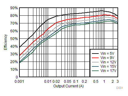
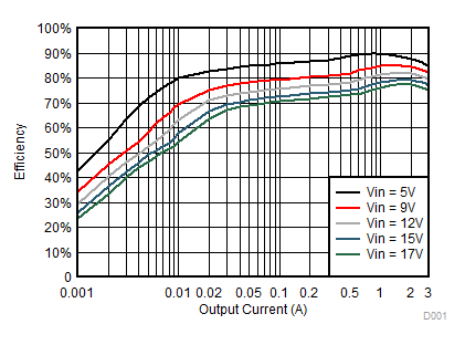
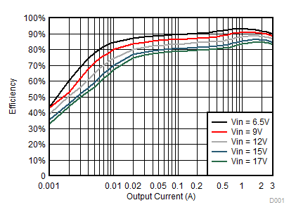
      2.      TPS563240 效率
  4. 修订历史记录
  5. Pin Configuration and Functions
    1.     Pin Functions
  6. Specifications
    1. 6.1 Absolute Maximum Ratings
    2. 6.2 ESD Ratings
    3. 6.3 Recommended Operating Conditions
    4. 6.4 Thermal Information
    5. 6.5 Electrical Characteristics
    6. 6.6 Typical Characteristics
  7. Detailed Description
    1. 7.1 Overview
    2. 7.2 Functional Block Diagram
    3. 7.3 Feature Description
      1. 7.3.1 Adaptive On-Time Control and PWM Operation
      2. 7.3.2 Pulse Skip Control
      3. 7.3.3 Out-of-Audio (OOA) Operation
      4. 7.3.4 Soft Start and Pre-Biased Soft Start
      5. 7.3.5 Current Protection
      6. 7.3.6 Undervoltage Lockout (UVLO) Protection
      7. 7.3.7 Thermal Shutdown
    4. 7.4 Device Functional Modes
      1. 7.4.1 Normal Operation
      2. 7.4.2 Eco-mode Operation
      3. 7.4.3 Standby Operation
  8. Application and Implementation
    1. 8.1 Application Information
    2. 8.2 Typical Application
      1. 8.2.1 Design Requirements
      2. 8.2.2 Detailed Design Procedure
        1. 8.2.2.1 Output Voltage Resistors Selection
        2. 8.2.2.2 Output Filter Selection
        3. 8.2.2.3 Input Capacitor Selection
        4. 8.2.2.4 Bootstrap Capacitor Selection
        5. 8.2.2.5 Dropout
      3. 8.2.3 Application Curves
  9. Power Supply Recommendations
  10. 10Layout
    1. 10.1 Layout Guidelines
    2. 10.2 Layout Example
  11. 11器件和文档支持
    1. 11.1 接收文档更新通知
    2. 11.2 社区资源
    3. 11.3 商标
    4. 11.4 静电放电警告
    5. 11.5 术语表
  12. 12机械、封装和可订购信息

封装选项

机械数据 (封装 | 引脚)
散热焊盘机械数据 (封装 | 引脚)
订购信息

Typical Characteristics

VIN = 12 V (unless otherwise noted)
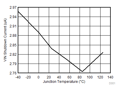
TPS563240 Ishutdown_SLVSE54.gif
Figure 1. Shutdown Current vs Junction Temperature
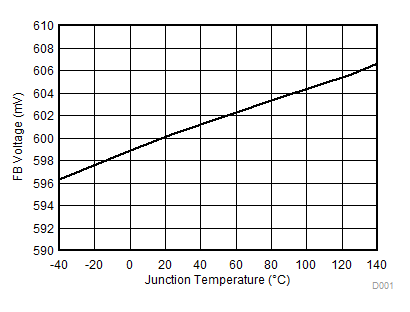
TPS563240 FB_Voltage_SLVSE54.gif
Figure 3. VFB Voltage vs Junction Temperature
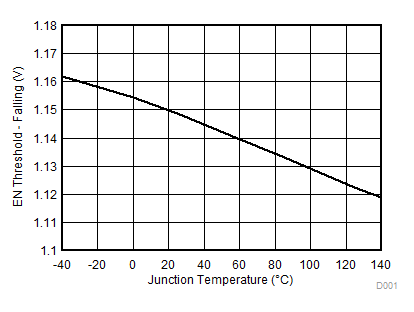
TPS563240 EN_Falling_SLVSE54.gif
Figure 5. EN Falling threshold vs Junction Temperature
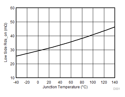
TPS563240 LowSideRdson_SLVSE54.gif
Figure 7. Low-Side Rds-On vs Junction Temperature
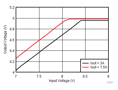
TPS563240 Dropout_5V_SLVSE74_2p0.gif
Figure 9. Dropout for 5 V Output Voltage
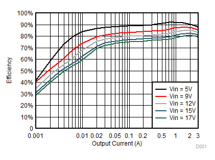
TPS563240 Eff_1.05V_SLVSE74_2p0.gif
1.05 V Efficiency L = 0.56 μH (Wurth:744383560056)
Figure 11. Efficiency vs Output Current, VOUT = 1.05 V
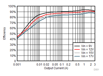
TPS563240 Eff_1.5V_SLVSE74_2p0.gif
1.5 V Efficiency L = 0.68 μH (Wurth:744383560068)
Figure 13. Efficiency vs Output Current, VOUT = 1.5 V
TPS563240 Eff_2.5V_SLVSE74_2p0.gif
2.5 V Efficiency L = 1 μH (Wurth:744311100)
Figure 15. Efficiency vs Output Current, VOUT = 2.5 V
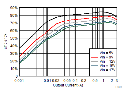
TPS563240 Eff_5V_SLVSE74_2p0.gif
5 V Efficiency L = 1.5 μH (Wurth:744311150)
Figure 17. Efficiency vs Output Current, VOUT = 5 V
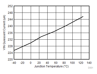
TPS563240 Iq_SLVSE74.gif
Figure 2. Supply Current vs Junction Temperature
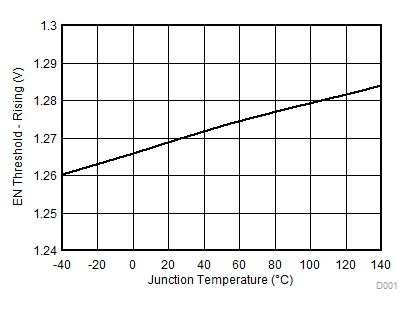
TPS563240 EN_Rising_SLVSE54.gif
Figure 4. EN Rising threshold vs Junction Temperature
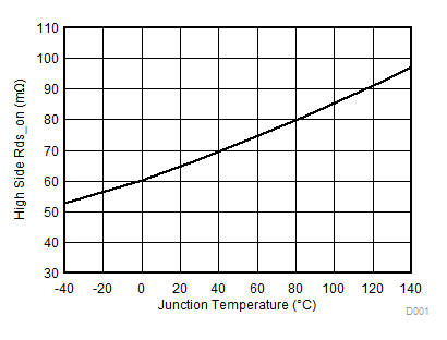
TPS563240 HighSideRdson_SLVSE54.gif
Figure 6. High-Side Rds-On vs Junction Temperature
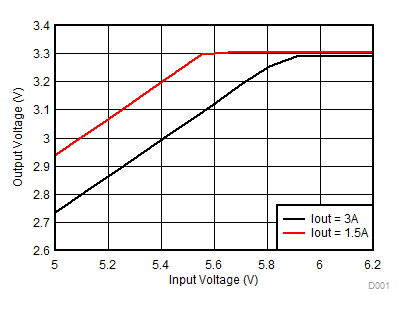
TPS563240 Dropout_3.3V_SLVSE74_2p0.gif
Figure 8. Dropout for 3.3 V Output Voltage
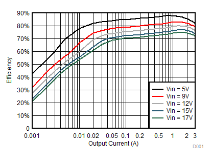
TPS563240 Eff_0.9V_SLVSE74_2p0.gif
0.9 V Efficiency L = 0.56 μH (Wurth:744383560056)
Figure 10. Efficiency vs Output Current, VOUT = 0.9 V
TPS563240 Eff_1.2V_SLVSE74_2p0.gif
1.2 V Efficiency L = 0.68 μH (Wurth:744383560068)
Figure 12. Efficiency vs Output Current, VOUT = 1.2 V
TPS563240 Eff_1.8V_SLVSE74_2p0.gif
1.8 V Efficiency L = 1 μH (Wurth:744311100)
Figure 14. Efficiency vs Output Current, VOUT = 1.8 V
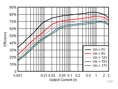
TPS563240 Eff_3.3V_SLVSE74_2p0.gif
3.3 V Efficiency L = 1.5 μH (Wurth:744311150)
Figure 16. Efficiency vs Output Current, VOUT = 3.3 V