ZHCSJ66 December 2018 TPS563240
PRODUCTION DATA.
7.3.3 Out-of-Audio™ (OOA) Operation
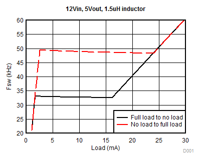
As the load current continues to decrease, the switching frequency can decrease into the acoustic audible frequency range. To prevent this from happening, Out-of-Audio™ (OOA) operation under light-load condition is implemented. The OOA control circuit monitors the states of both the high-side and low-side FETs. When both high-side and low-side FETs are off for a period longer than 30 μs, the on time generated by one shot timer is decreased by a little step, thus the off time of both FETs will be reduced to a length lower than 30us. If the load current decreases further, and cause the off time of both FETs longer than 30us again, the above described on time reduction process will repeat. By this means, the switching frequency is maintained higher than ~33kHz as load decrease. When the on time reduces to ~30% of that in CCM operation, the on time will keep at this minimum length. If load current decreases further, the switching frequency can't be maintained at ~33kHz anymore, instead, it will decrease linearly towards zero.
When the load current increases from zero, the on time is kept at minimum length, which is~30% of that in CCM operation, and the switching frequency increases linearly as load increases. When the off time of both FETs decreases to a length lower than 20us, the on time generated by one shot timer will increase by a step, thus the off time of both FETs will be increased above 20us. If the load current increases further, and cause the off time of both FETs shorter than 20us again, the above described on time increase process will repeat. By this means, the switching frequency is maintained lower than ~50kHz as load increases. When the on time increases to the length of that in CCM operation, the on time can't be increased anymore. If load current continue increases, the switching frequency will increase linearly towards 1.4MHz nominal frequency. Below figure shows the frequency VS load curve at 12Vin/5Vout condition with 1.5uH inductor used.
 Figure 18. Frequency VS load current at 12Vin/5Vout condition with 1.5uH inductor used