ZHCSJ66 December   2018 TPS563240

PRODUCTION DATA.  

  1. 特性
  2. 应用
  3. 说明
    1.     Device Images
      1.      简化电路原理图
      2.      TPS563240 效率
  4. 修订历史记录
  5. Pin Configuration and Functions
    1.     Pin Functions
  6. Specifications
    1. 6.1 Absolute Maximum Ratings
    2. 6.2 ESD Ratings
    3. 6.3 Recommended Operating Conditions
    4. 6.4 Thermal Information
    5. 6.5 Electrical Characteristics
    6. 6.6 Typical Characteristics
  7. Detailed Description
    1. 7.1 Overview
    2. 7.2 Functional Block Diagram
    3. 7.3 Feature Description
      1. 7.3.1 Adaptive On-Time Control and PWM Operation
      2. 7.3.2 Pulse Skip Control
      3. 7.3.3 Out-of-Audio (OOA) Operation
      4. 7.3.4 Soft Start and Pre-Biased Soft Start
      5. 7.3.5 Current Protection
      6. 7.3.6 Undervoltage Lockout (UVLO) Protection
      7. 7.3.7 Thermal Shutdown
    4. 7.4 Device Functional Modes
      1. 7.4.1 Normal Operation
      2. 7.4.2 Eco-mode Operation
      3. 7.4.3 Standby Operation
  8. Application and Implementation
    1. 8.1 Application Information
    2. 8.2 Typical Application
      1. 8.2.1 Design Requirements
      2. 8.2.2 Detailed Design Procedure
        1. 8.2.2.1 Output Voltage Resistors Selection
        2. 8.2.2.2 Output Filter Selection
        3. 8.2.2.3 Input Capacitor Selection
        4. 8.2.2.4 Bootstrap Capacitor Selection
        5. 8.2.2.5 Dropout
      3. 8.2.3 Application Curves
  9. Power Supply Recommendations
  10. 10Layout
    1. 10.1 Layout Guidelines
    2. 10.2 Layout Example
  11. 11器件和文档支持
    1. 11.1 接收文档更新通知
    2. 11.2 社区资源
    3. 11.3 商标
    4. 11.4 静电放电警告
    5. 11.5 术语表
  12. 12机械、封装和可订购信息

封装选项

机械数据 (封装 | 引脚)
散热焊盘机械数据 (封装 | 引脚)
订购信息

Pin Configuration and Functions

DDC Package
6-Pin SOT
Top View
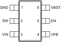
TPS563240 Pinout_DDC-6_SLVSD90.gif

Pin Functions

PIN I/O DESCRIPTION
NAME NO.
GND 1 Ground pin Source terminal of low-side power NFET as well as the ground terminal for controller circuit. Connect sensitive VFB to this GND at a single point.
SW 2 O Switch node connection between high-side NFET and low-side NFET.
VIN 3 I Input voltage supply pin. The drain terminal of high-side power NFET.
VFB 4 I Converter feedback input. Connect to output voltage with feedback resistor divider.
EN 5 I Enable input control. Active high and must be pulled up to enable the device.
VBST 6 O Supply input for the high-side NFET gate drive circuit. Connect 0.1 µF capacitor between VBST and SW pins.