ZHCSJ24A November   2018  – May 2019 TPS56339

PRODUCTION DATA.  

  1. 特性
  2. 应用
  3. 说明
    1.     Device Images
      1.      简化原理图
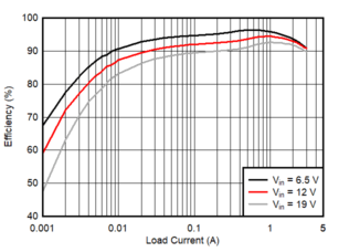
      2.      TPS56339 效率
  4. 修订历史记录
  5. Pin Configuration and Functions
    1.     Pin Functions
  6. Specifications
    1. 6.1 Absolute Maximum Ratings
    2. 6.2 ESD Ratings
    3. 6.3 Recommended Operating Conditions
    4. 6.4 Thermal Information
    5. 6.5 Electrical Characteristics
    6. 6.6 Timing Requirements
    7. 6.7 Typical Characteristics
  7. Detailed Description
    1. 7.1 Overview
    2. 7.2 Functional Block Diagram
    3. 7.3 Feature Description
      1. 7.3.1 Advanced Emulated Current Mode Control
      2. 7.3.2 Enable and Adjusting Undervoltage Lockout
      3. 7.3.3 Soft Start and Pre-Biased Soft Start
      4. 7.3.4 Voltage Reference
      5. 7.3.5 Minimum ON-time, Minimum OFF-time and Frequency Foldback at Dropout Conditions
      6. 7.3.6 Overcurrent and Undervoltage Protection
      7. 7.3.7 Thermal Shutdown
    4. 7.4 Device Functional Modes
      1. 7.4.1 Shutdown Mode
      2. 7.4.2 Active Mode
      3. 7.4.3 CCM Operation
    5. 7.5 Light-Load Operation
  8. Application and Implementation
    1. 8.1 Application Information
    2. 8.2 Typical Application
      1. 8.2.1 Design Requirements
      2. 8.2.2 Detailed Design Procedure
        1. 8.2.2.1 Custom Design With WEBENCH® Tools
        2. 8.2.2.2 Output Voltage Resistors Selection
        3. 8.2.2.3 Output Inductor Selection
        4. 8.2.2.4 Output Capacitor Selection
        5. 8.2.2.5 Input Capacitor Selection
        6. 8.2.2.6 Bootstrap Capacitor Selection
      3. 8.2.3 Undervoltage Lockout Set Point
      4. 8.2.4 Application Curves
  9. Power Supply Recommendations
  10. 10Layout
    1. 10.1 Layout Guidelines
    2. 10.2 Layout Example
  11. 11器件和文档支持
    1. 11.1 接收文档更新通知
    2. 11.2 相关链接
    3. 11.3 社区资源
    4. 11.4 商标
    5. 11.5 静电放电警告
    6. 11.6 Glossary
  12. 12机械、封装和可订购信息

封装选项

机械数据 (封装 | 引脚)
散热焊盘机械数据 (封装 | 引脚)
订购信息

Typical Characteristics

VIN = 12 V (unless otherwise noted)
TPS56339 D001_SLVSEI2.gif
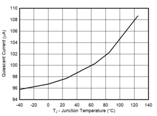
Figure 1. Quiescent Current VS Junction Temperature
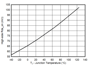
TPS56339 D003_SLVSEI2.gif
Figure 3. High-side Rds-On VS Junction Temperature
TPS56339 D005_SLVSEI2.gif
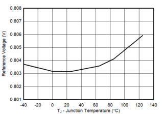
Figure 5. Reference Voltage VS Junction Temperature
TPS56339 D007_SLVSEI2.gif
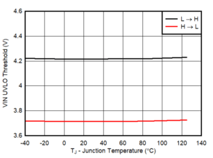
Figure 7. VIN UVLO Threshold VS Junction Temperature
TPS56339 D009_SLVSEI2.gif
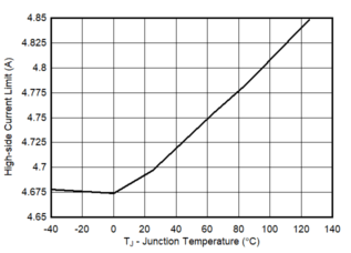
Figure 9. High-side Current Limit Threshold VS Junction Temperature
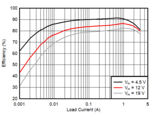
TPS56339 Eff-1.05V_SLVSEI2.gif
Figure 11. VOUT=1.05 V Efficiency, L=1.5 µH
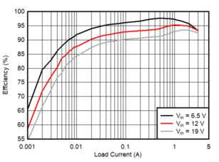
TPS56339 Eff-5V_SLVSEI2.gif
Figure 13. VOUT=5 V Efficiency, L=5.6 µH
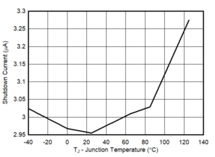
TPS56339 D002_SLVSEI2.gif
Figure 2. Shutdown Current VS Junction Temperature
TPS56339 D004_SLVSEI2.gif
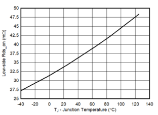
Figure 4. Low-side Rds-On VS Junction Temperature
TPS56339 D006_SLVSEI2.gif
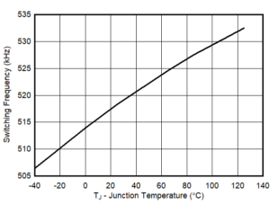
Figure 6. Switching Frequency VS Junction Temperature
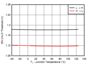
TPS56339 D008_SLVSEI2.gif
Figure 8. EN Threshold VS Junction Temperature
TPS56339 D010_SLVSEI2.gif
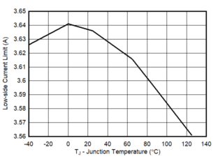
Figure 10. Low-side Current Limit Threshold VS Junction Temperature
TPS56339 Eff-3.3V_SLVSEI2.gif
Figure 12. VOUT=3.3 V Efficiency, L=4.7 µH
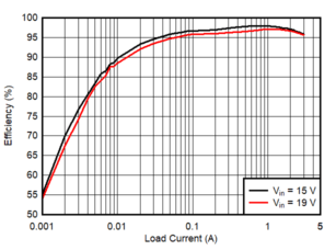
TPS56339 Eff-12V_SLVSEI2.gif
Figure 14. VOUT=12 V Efficiency, L=6.8 µH