ZHCSLD3B May   2020  – December 2023 TPS566231 , TPS566238

PRODUCTION DATA  

  1.   1
  2. 特性
  3. 应用
  4. 说明
  5. Pin Configuration and Functions
  6. Specifications
    1. 5.1 Absolute Maximum Ratings
    2. 5.2 ESD Ratings
    3. 5.3 Recommended Operating Conditions
    4. 5.4 Thermal Information
    5. 5.5 Electrical Characteristics
    6. 5.6 Typical Characteristics
  7. Detailed Description
    1. 6.1 Overview
    2. 6.2 Functional Block Diagram
    3. 6.3 Feature Description
      1. 6.3.1 PWM Operation and D-CAP3™ Control Mode
      2. 6.3.2 Soft Start
      3. 6.3.3 Power Good
      4. 6.3.4 Large Duty Operation
      5. 6.3.5 Overcurrent Protection and Undervoltage Protection
      6. 6.3.6 Overvoltage Protection
      7. 6.3.7 UVLO Protection
      8. 6.3.8 Output Voltage Discharge
      9. 6.3.9 Thermal Shutdown
    4. 6.4 Device Functional Modes
      1. 6.4.1 Advanced Eco-mode Control
      2. 6.4.2 Force CCM Mode
      3. 6.4.3 Standby Operation
  8. Application and Implementation
    1. 7.1 Application Information
    2. 7.2 Typical Application
      1. 7.2.1 Design Requirements
      2. 7.2.2 Detailed Design Procedure
        1. 7.2.2.1 Custom Design with WEBENCH® Tools
        2. 7.2.2.2 Output Voltage Setpoint
        3. 7.2.2.3 Inductor Selection
        4. 7.2.2.4 Output Capacitor Selection
        5. 7.2.2.5 Input Capacitor Selection
      3. 7.2.3 Application Curves
    3. 7.3 Power Supply Recommendations
    4. 7.4 Layout
      1. 7.4.1 Layout Guidelines
      2. 7.4.2 Layout Example
  9. Device and Documentation Support
    1. 8.1 Device Support
      1. 8.1.1 Development Support
        1. 8.1.1.1 Custom Design with WEBENCH® Tools
    2. 8.2 接收文档更新通知
    3. 8.3 支持资源
    4. 8.4 Trademarks
    5. 8.5 静电放电警告
    6. 8.6 术语表
  10. Revision History
  11. 10Mechanical, Packaging, and Orderable Information

封装选项

机械数据 (封装 | 引脚)
散热焊盘机械数据 (封装 | 引脚)
订购信息

Application Curves

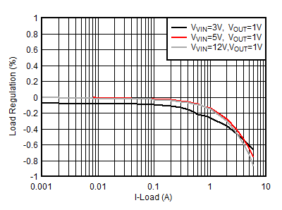
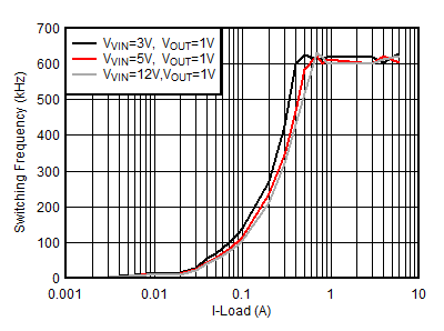
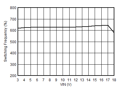
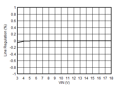
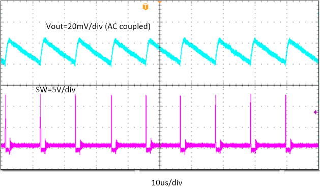
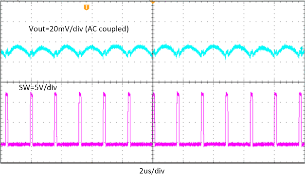
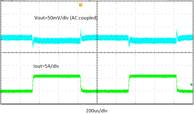
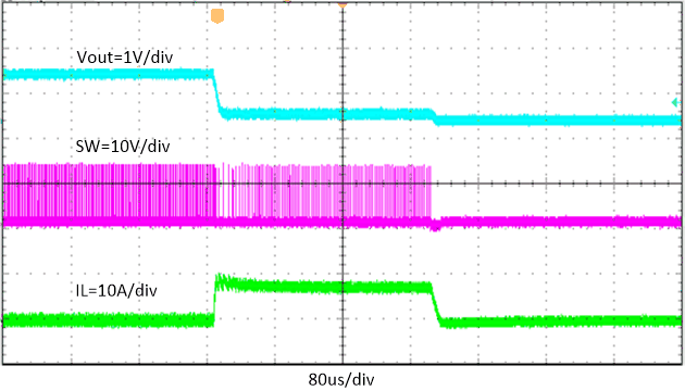
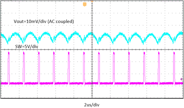
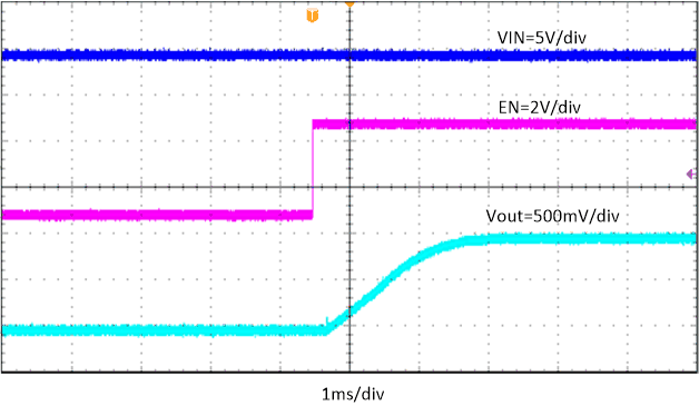
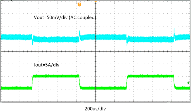
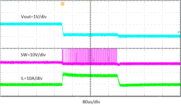
Figure 7-2 through Figure 7-25 apply to the circuit of Figure 7-1. VIN = 12 V, TA = 25°C unless otherwise specified.
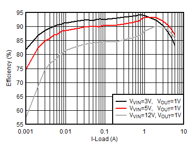
GUID-D3938889-6804-4E89-B8C5-386E2B896831-low.gifFigure 7-2 TPS566231 Efficiency Curve
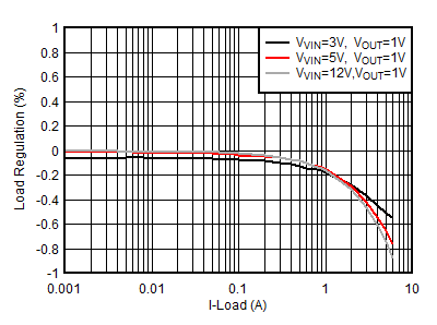
GUID-66A7D734-A3A1-4C3E-A4E4-934688752F55-low.gifFigure 7-4 TPS566231 Load Regulation
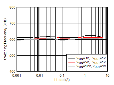
GUID-D94C32B6-B7DF-497F-BE46-B0B454A4DEAA-low.gifFigure 7-6 TPS566231 FSW vs Output Load
GUID-20201230-CA0I-BMZ9-SDVT-MFQTM2LHZSRQ-low.gif
IOUT = 6 A
Figure 7-8 Switching Frequency vs Input Voltage
GUID-20201230-CA0I-TQFS-KKBS-X1GPQPGH8MMD-low.gif
IOUT = 0.1 A
Figure 7-10 TPS566238 Line Regulation
GUID-E660C6AA-445C-41DC-B292-30D568FEDF03-low.gif
IOUT = 0.01 A
Figure 7-12 TPS566231 Output Voltage Ripple
GUID-B4F68E94-AB65-4A46-8122-7FB72E3E6D4F-low.gifFigure 7-14 Output Voltage Ripple, IOUT = 6 A
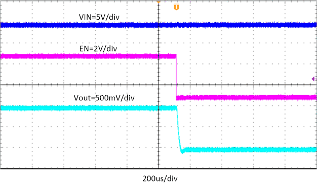
GUID-926233FE-79BF-41C7-889E-0CF3E332B9E5-low.gifFigure 7-16 Shutdown Through EN, IOUT = 3 A
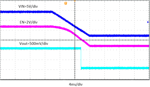
GUID-11BCB862-55E6-4051-A082-877F6172F950-low.gifFigure 7-18 Start-Up with VIN Falling, IOUT = 3 A
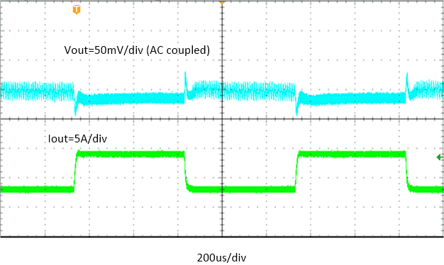
GUID-2A8EFFD1-34F6-4A52-8ADE-4B00175FEBAA-low.gif
0.1 A to 6 A Slew Rate = 2.5 A/μs
Figure 7-20 TPS566231 Transient Response
GUID-41105268-68D2-4DFF-B0BD-FFB4081D51C0-low.gif
0.1 A to 6 A Slew Rate = 2.5 A/μs
Figure 7-22 TPS566238 Transient Response
GUID-818E3BE5-1A61-41E8-BE7C-581F8F0BF8C0-low.gifFigure 7-24 TPS566238 Normal Operation to Output Hard Short
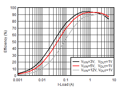
GUID-881689E9-B846-44FC-9AF8-E3DC8FC36CA5-low.gifFigure 7-3 TPS566238 Efficiency Curve
GUID-3BD4716F-6476-4A52-A6DD-C35D36C95740-low.gifFigure 7-5 TPS566238 Load Regulation
GUID-C429AFD9-F413-4586-95D1-A58BD6EAA0F7-low.gifFigure 7-7 TPS566238 FSW vs Output Load
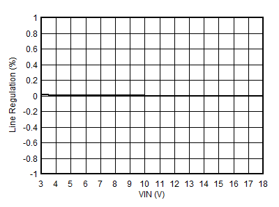
GUID-20201230-CA0I-KJVZ-FQPP-7SCGPWHZ91GL-low.gif
IOUT = 0.1 A 
Figure 7-9 TPS566231 Line Regulation
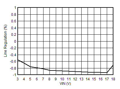
GUID-20201230-CA0I-9BMJ-W3DH-XV3B7HH048HM-low.gif
IOUT = 6 A
Figure 7-11 Line Regulation
GUID-BA931773-52CA-492E-AD17-7EDAD410A85F-low.gif
IOUT = 0.01 A
Figure 7-13 TPS566238 Output Voltage Ripple
GUID-A7DE4647-313B-4802-883A-B68B71FECB8D-low.gifFigure 7-15 Start-Up Through EN, IOUT = 3 A
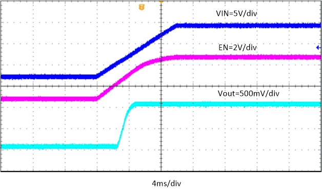
GUID-695B3C73-CEA6-4D47-ACFD-7A6645C55C75-low.gifFigure 7-17 Start-Up with VIN Rising, IOUT = 3 A
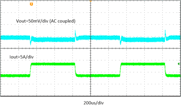
GUID-7668F3E4-D07C-4939-A56F-F8A4C5564ED0-low.gif
0.6 A to 5.4 A Slew Rate = 2.5 A/μs
Figure 7-19 TPS566231 Transient Response
GUID-CBDA630B-95A2-440B-9FA2-B189F4777EA6-low.gif
0.6 A to 5.4 A Slew Rate = 2.5 A/μs
Figure 7-21 TPS566238 Transient Response
GUID-10761E81-462F-4137-BC11-D8BC9732F938-low.gifFigure 7-23 TPS566231 Normal Operation to Output Hard Short
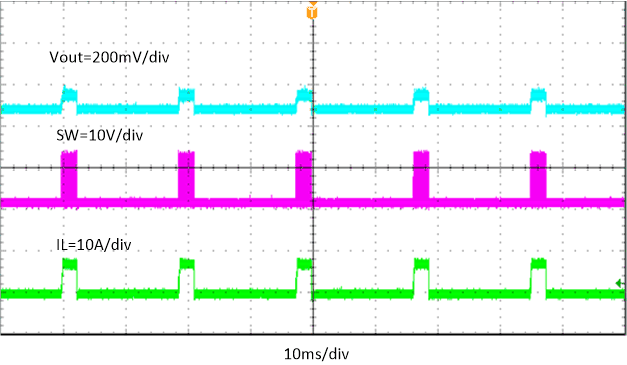
GUID-41F2746E-CC76-4B2D-A339-82A18A6487D7-low.gifFigure 7-25 Output Hard Short Hiccup