ZHCSJL9B April   2019  – April 2019 TPS566235

PRODUCTION DATA.  

  1. 特性
  2. 应用
  3. 说明
    1.     Device Images
      1.      典型应用
      2.      效率与输出电流 Eco-mode
  4. 修订历史记录
  5. Pin Configuration and Functions
    1.     Pin Functions
  6. Specifications
    1. 6.1 Absolute Maximum Ratings
    2. 6.2 ESD Ratings
    3. 6.3 Recommended Operating Conditions
    4. 6.4 Thermal Information
    5. 6.5 Electrical Characteristics
    6. 6.6 Typical Characteristics
  7. Detailed Description
    1. 7.1 Overview
    2. 7.2 Functional Block Diagram
    3. 7.3 Feature Description
      1. 7.3.1 PWM Operation and D-CAP3 Control
      2. 7.3.2 Power Good
      3. 7.3.3 Soft Start and Pre-Biased Soft Start
      4. 7.3.4 Over current Protection and Undervoltage Protection
      5. 7.3.5 Over Voltage Protection
      6. 7.3.6 UVLO Protection
      7. 7.3.7 Thermal Shutdown
    4. 7.4 Device Functional Modes
      1. 7.4.1 Light Load Operation
      2. 7.4.2 MODE Pin Configuration
      3. 7.4.3 Advanced Eco-Mode Control
      4. 7.4.4 Out-Of-Audio Mode
      5. 7.4.5 Force CCM Mode
      6. 7.4.6 Standby Operation
  8. Application and Implementation
    1. 8.1 Application Information
    2. 8.2 Typical Application
      1. 8.2.1 Design Requirements
      2. 8.2.2 Detailed Design Procedure
        1. 8.2.2.1 Custom Design With WEBENCH® Tools
        2. 8.2.2.2 Inductor Selection
        3. 8.2.2.3 Output Capacitor Selection
        4. 8.2.2.4 Input Capacitor Selection
      3. 8.2.3 Application Curves
  9. Power Supply Recommendations
  10. 10Layout
    1. 10.1 Layout Guidelines
    2. 10.2 Layout Example
  11. 11器件和文档支持
    1. 11.1 器件支持
      1. 11.1.1 第三方米6体育平台手机版_好二三四免责声明
      2. 11.1.2 开发支持
        1. 11.1.2.1 使用 WEBENCH® 工具创建定制设计
    2. 11.2 接收文档更新通知
    3. 11.3 社区资源
    4. 11.4 商标
    5. 11.5 静电放电警告
    6. 11.6 术语表
  12. 12机械、封装和可订购信息

封装选项

机械数据 (封装 | 引脚)
散热焊盘机械数据 (封装 | 引脚)
订购信息

MODE Pin Configuration

TPS566235 detect the voltage on the MODE pin during start-up and latches onto one of the MODE options listed below in Table 1. TPS566235 internally has a comparator to compare this voltage with reference voltage and decide which mode to choose. The voltage on the MODE pin can be set by connecting to VCC pin or connecting a resistor RM between this pin and AGND. There is a source current of 5 µA at the mode pin and generate voltage for mode selection to avoid noise and spurious trigger. The VMODE voltage range and recommended resistor value is shown in Table 1. The MODE pin setting can be reset only by VIN power cycling or EN toggle.

Table 1. Mode Pin Settings

VMODE 0-0.3 V 0.3 V-1.2 V >1.2 V
Recommended Resistor 0 Ω 100 kΩ-150 kΩ To VCC (recommend) or RM>400kΩ
Operating Mode Eco-Mode™ OOA FCCM

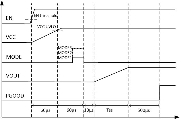
Figure 18 shows the typical start-up sequence of the device once the enable signal crosses the EN turn on threshold (VIN is higher then UVLO threshold). After the voltage on VCC crosses the rising UVLO threshold, it takes about 60 µs to read the mode setting .The output voltage starts ramping after 10 µs from the mode reading is done.
TPS566235 fbd-03-slvsew1.gifFigure 18. Start-Up Sequence