ZHCSIH1A July 2018 – September 2019 TPS56637
PRODUCTION DATA.
- 1 特性
- 2 应用
- 3 说明
- 4 修订历史记录
- 5 Pin Configuration and Functions
- 6 Specifications
-
7 Detailed Description
- 7.1 Overview
- 7.2 Functional Block Diagram
- 7.3
Feature Description
- 7.3.1 The Adaptive On-Time Control and PWM Operation
- 7.3.2 Mode Selection
- 7.3.3 Soft Start and Pre-Biased Soft Start
- 7.3.4 Enable and Adjusting Undervoltage Lockout
- 7.3.5 Output Overcurrent Limit and Undervoltage Protection
- 7.3.6 Overvoltage Protection
- 7.3.7 UVLO Protection
- 7.3.8 Thermal Shutdown
- 7.3.9 Output Voltage Discharge
- 7.3.10 Power Good
- 7.4 Device Functional Modes
- 8 Application and Implementation
- 9 Power Supply Recommendations
- 10Layout
- 11器件和文档支持
- 12机械、封装和可订购信息
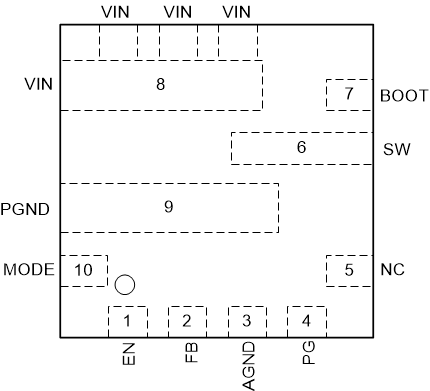
5 Pin Configuration and Functions
RPA Package
10-Pin VQFN-HR
Top View

Pin Functions
| PIN | TYPE | DESCRIPTION | |
|---|---|---|---|
| NAME | NO. | ||
| AGND | 3 | G | Ground of internal analog circuitry. Connect AGND to PGND plane at a single point. |
| BOOT | 7 | I | Supply input for the gate drive voltage of the high-side MOSFET. Connect a 0.1-µF bootstrap capacitor between BOOT and SW. |
| EN | 1 | I | Enable input control. Driving EN high or leaving this pin floating enables the converter. A resistor divider can be used to imply an UVLO function. |
| FB | 2 | I | Output feedback. Connect FB to the tap of an external resistor divider from the output to GND to set the output voltage. |
| MODE | 10 | I | Operation mode selection pin. Leaving this pin floating(≥500 kΩ) forces the TPS56637 into FCCM. Connecting this pin to GND(≤10 kΩ) forces the TPS56637 into Eco-mode™ under light load. |
| NC | 5 | N | Not Connected, keep this pin floating. |
| PG | 4 | O | Open Drain Power Good Indicator, it is asserted low if output voltage is out of PG threshold due to over-voltage, under-voltage, thermal shutdown, EN shutdown or during soft-start. |
| PGND | 9 | G | Power GND terminal. Source terminal of low side MOSFET. |
| SW | 6 | O | Switching node terminal. Connect the output inductor to this pin with wide and short tracks |
| VIN | 8 | P | Input voltage supply pin. Drain terminal of high-side MOSFET. Connect the input decoupling capacitors between VIN and GND. |