ZHCSEU8G March 2016 – August 2024 TPS56C215
PRODUCTION DATA
- 1
- 1 特性
- 2 应用
- 3 说明
- 4 Pin Configuration and Functions
- 5 Specifications
-
6 Detailed Description
- 6.1 Overview
- 6.2 Functional Block Diagram
- 6.3
Feature Description
- 6.3.1 PWM Operation and D-CAP3™ Control Mode
- 6.3.2 Eco-mode Control
- 6.3.3 4.7-V LDO
- 6.3.4 MODE Selection
- 6.3.5 Soft Start and Prebiased Soft Start
- 6.3.6 Enable and Adjustable UVLO
- 6.3.7 Power Good
- 6.3.8 Overcurrent Protection and Undervoltage Protection
- 6.3.9 UVLO Protection
- 6.3.10 Thermal Shutdown
- 6.3.11 Output Voltage Discharge
- 6.4 Device Functional Modes
- 7 Application and Implementation
- 8 Device and Documentation Support
- 9 Revision History
- 10Mechanical, Packaging, and Orderable Information
6.3.4 MODE Selection
The TPS56C215 has a MODE pin that can offer 12 different states of operation as a combination of current limit, switching frequency, and light load operation. The device can operate at two different current limits ILIM-1 and ILIM to support an output continuous current of 10 A and 12 A, respectively. The TPS56C215 is designed to compare the valley current of the inductor against the current limit thresholds so understand that the output current is half the ripple current higher than the valley current. For example, with the ILIM current limit selection, the OCL threshold is 11.73-A minimum, which means that a pk-pk inductor ripple current of 0.54-A minimum is needed to be able to draw 12 A out of the converter without entering an overcurrent condition. The TPS56C215 can operate at three different frequencies of 400 kHz, 800 kHz, and 1200 kHz and also can choose between Eco-mode and FCCM mode. The device reads the voltage on the MODE pin during start-up and latches onto one of the MODE options listed in Table 6-3. The voltage on the MODE pin can be set by connecting this pin to the center tap of a resistor divider connected between VREG5 and AGND. A guideline for the top resistor (RM_H) and the bottom resistor (RM_L) in 1% resistors is shown in Table 6-3. It is important that the voltage for the MODE pin is derived from the VREG5 rail only because internally this voltage is referenced to detect the MODE option. The MODE pin setting can be reset only by a VIN power cycling.
| RM_L (kΩ) | RM_H (kΩ) | LIGHT LOAD OPERATION | CURRENT LIMIT | FREQUENCY (kHz) |
|---|---|---|---|---|
| 5.1 | 300 | FCCM | ILIM-1 | 400 |
| 10 | 200 | FCCM | ILIM | 400 |
| 20 | 160 | FCCM | ILIM-1 | 800 |
| 20 | 120 | FCCM | ILIM | 800 |
| 51 | 200 | FCCM | ILIM-1 | 1200 |
| 51 | 180 | FCCM | ILIM | 1200 |
| 51 | 150 | DCM | ILIM-1 | 400 |
| 51 | 120 | DCM | ILIM | 400 |
| 51 | 91 | DCM | ILIM-1 | 800 |
| 51 | 82 | DCM | ILIM | 800 |
| 51 | 62 | DCM | ILIM-1 | 1200 |
| 51 | 51 | DCM | ILIM | 1200 |
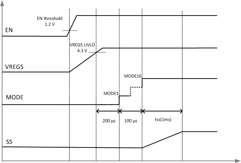
Figure 6-2 shows the typical start-up sequence of the device after the EN pin voltage crosses the EN turn-on threshold. After the voltage on VREG5 pin crosses the rising UVLO threshold, it takes 100 μs to read the first MODE setting and approximately 100 μs from there to finish the last MODE setting. The output voltage starts ramping after the MODE setting reading is completed.
 Figure 6-2 Power-Up Sequence