ZHCSEU8G March 2016 – August 2024 TPS56C215
PRODUCTION DATA
- 1
- 1 特性
- 2 应用
- 3 说明
- 4 Pin Configuration and Functions
- 5 Specifications
-
6 Detailed Description
- 6.1 Overview
- 6.2 Functional Block Diagram
- 6.3
Feature Description
- 6.3.1 PWM Operation and D-CAP3™ Control Mode
- 6.3.2 Eco-mode Control
- 6.3.3 4.7-V LDO
- 6.3.4 MODE Selection
- 6.3.5 Soft Start and Prebiased Soft Start
- 6.3.6 Enable and Adjustable UVLO
- 6.3.7 Power Good
- 6.3.8 Overcurrent Protection and Undervoltage Protection
- 6.3.9 UVLO Protection
- 6.3.10 Thermal Shutdown
- 6.3.11 Output Voltage Discharge
- 6.4 Device Functional Modes
- 7 Application and Implementation
- 8 Device and Documentation Support
- 9 Revision History
- 10Mechanical, Packaging, and Orderable Information
7.2.3 Application Curves
Figure 7-2 through Figure 7-18 apply to the circuit of Figure 7-1. VIN = 12 V. Ta = 25°C unless otherwise specified.
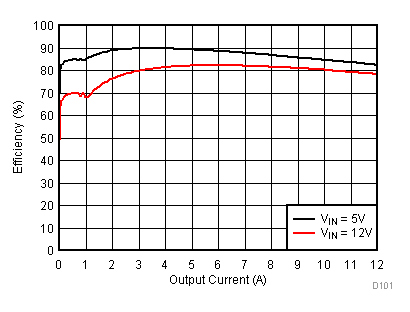 Figure 7-2 Efficiency
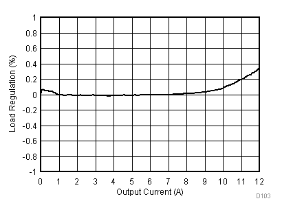 Figure 7-4 Load
Regulation, VIN = 5 V
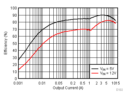 Figure 7-3 Light
Load Efficiency
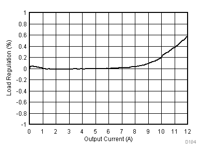 Figure 7-5 Load
Regulation, VIN = 12 V
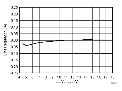 Figure 7-6 Line
Regulation, IOUT = 6 A
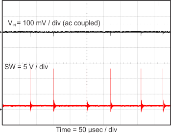 Figure 7-8 Input
Voltage Ripple, IOUT = 10 mA
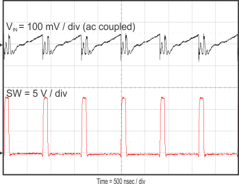 Figure 7-10 Input
Voltage Ripple, IOUT = 12 A
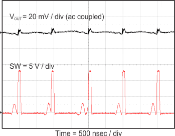 Figure 7-12 Output Voltage Ripple, IOUT = 800 mA
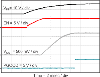 Figure 7-14 Start
Up Relative to VIN Rising
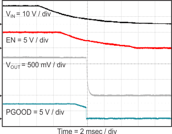 Figure 7-16 Shut
Down Relative to VIN Falling
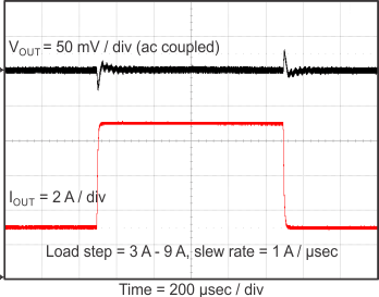 Figure 7-18 Transient Response
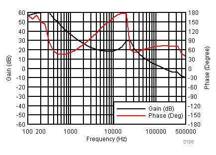 Figure 7-7 Loop
Response, IOUT = 6 A
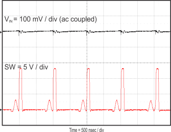 Figure 7-9 Input
Voltage Ripple, IOUT = 800 mA
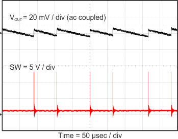 Figure 7-11 Output Voltage Ripple, IOUT = 10 mA
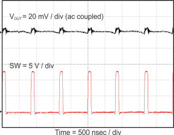 Figure 7-13 Output Voltage Ripple, IOUT = 12 A
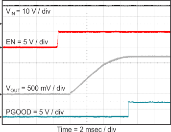 Figure 7-15 Start
Up Relative to EN Rising
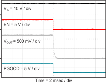 Figure 7-17 Shut
Down Relative to EN Falling