ZHCS026C December 2010 – February 2016 TPS57060-Q1
PRODUCTION DATA.
- 1 特征
- 2 应用
- 3 说明
- 4 修订历史记录
- 5 Pin Configuration and Functions
- 6 Specifications
-
7 Detailed Description
- 7.1 Overview
- 7.2 Functional Block Diagram
- 7.3
Feature Description
- 7.3.1 Fixed Frequency PWM Control
- 7.3.2 Slope Compensation Output Current
- 7.3.3 Low Dropout Operation and Bootstrap Voltage (BOOT)
- 7.3.4 Error Amplifier
- 7.3.5 Voltage Reference
- 7.3.6 Adjusting the Output Voltage
- 7.3.7 Enable and Adjusting Undervoltage Lockout (UVLO)
- 7.3.8 Slow Start and Tracking Pin (SS/TR)
- 7.3.9 Overload Recovery Circuit
- 7.3.10 Constant Switching Frequency and Timing Resistor (RT/CLK Pin)
- 7.3.11 Overcurrent Protection and Frequency Shift
- 7.3.12 Selecting the Switching Frequency
- 7.3.13 How to Interface to RT/CLK Pin
- 7.3.14 Power Good (PWRGD Pin)
- 7.3.15 Overvoltage Transient Protection
- 7.3.16 Thermal Shutdown
- 7.3.17 Small Signal Model for Loop Response
- 7.3.18 Simple Small-Signal Model for Peak Current-Mode Control
- 7.3.19 Small Signal Model for Frequency Compensation
- 7.4 Device Functional Modes
-
8 Application and Implementation
- 8.1 Application Information
- 8.2
Typical Application
- 8.2.1 Design Requirements
- 8.2.2
Detailed Design Procedure
- 8.2.2.1 Selecting the Switching Frequency
- 8.2.2.2 Output Inductor Selection (LO)
- 8.2.2.3 Output Capacitor
- 8.2.2.4 Catch Diode
- 8.2.2.5 Input Capacitor
- 8.2.2.6 Slow Start Capacitor
- 8.2.2.7 Bootstrap Capacitor Selection
- 8.2.2.8 Undervoltage Lockout Set Point
- 8.2.2.9 Output Voltage and Feedback Resistors Selection
- 8.2.2.10 Compensation
- 8.2.2.11 Discontinuous Mode and Eco Mode Boundary
- 8.2.3 Application Curves
- 9 Power Supply Recommendations
- 10Layout
- 11器件和文档支持
- 12机械、封装和可订购信息
封装选项
机械数据 (封装 | 引脚)
散热焊盘机械数据 (封装 | 引脚)
订购信息
7.3.7 Enable and Adjusting Undervoltage Lockout (UVLO)
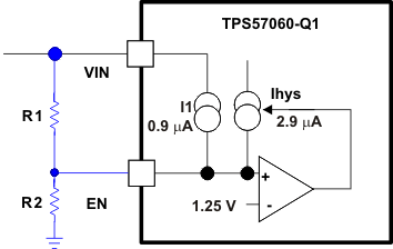
The TPS57060-Q1 device is disabled when the VIN pin voltage falls below 2.5 V. If an application requires a higher undervoltage lockout (UVLO), use the EN pin as shown in Figure 27 to adjust the input voltage UVLO by using the two external resistors. Although using the UVLO adjust registers is not is not required, consistent power-up behavior is highly recommended for operation. The EN pin has an internal pullup current source, I1, of 0.9 μA that provides the default condition of the TPS57060-Q1 device operating when the EN pin floats. When the EN pin voltage exceeds 1.25 V, an additional 2.9 μA of hysteresis, Ihys, is added. This additional current facilitates input voltage hysteresis. Use Equation 2 to set the external hysteresis for the input voltage. Use Equation 3 to set the input start voltage.
 Figure 27. Adjustable Undervoltage Lockout (UVLO)

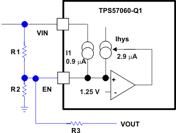
Another technique to add input voltage hysteresis is shown in Figure 28. This method may be used, if the resistance values are high from the previous method and a wider voltage hysteresis is needed. The resistor R3 sources additional hysteresis current into the EN pin.
 Figure 28. Adding Additional Hysteresis

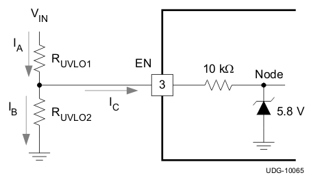
Do not place a low-impedance voltage source with greater than 5 V directly on the EN pin. Do not place a capacitor directly on the EN pin if VEN > 5 V when using a voltage divider to adjust the start and stop voltage. The node voltage, (see Figure 29) must remain equal to or less than 5.8 V. The zener diode can sink up to 100 μA. The EN pin voltage can be greater than 5 V if the VIN voltage source has a high impedance and does not source more than 100 μA into the EN pin.
 Figure 29. Node Voltage