ZHCS026C December 2010 – February 2016 TPS57060-Q1
PRODUCTION DATA.
- 1 特征
- 2 应用
- 3 说明
- 4 修订历史记录
- 5 Pin Configuration and Functions
- 6 Specifications
-
7 Detailed Description
- 7.1 Overview
- 7.2 Functional Block Diagram
- 7.3
Feature Description
- 7.3.1 Fixed Frequency PWM Control
- 7.3.2 Slope Compensation Output Current
- 7.3.3 Low Dropout Operation and Bootstrap Voltage (BOOT)
- 7.3.4 Error Amplifier
- 7.3.5 Voltage Reference
- 7.3.6 Adjusting the Output Voltage
- 7.3.7 Enable and Adjusting Undervoltage Lockout (UVLO)
- 7.3.8 Slow Start and Tracking Pin (SS/TR)
- 7.3.9 Overload Recovery Circuit
- 7.3.10 Constant Switching Frequency and Timing Resistor (RT/CLK Pin)
- 7.3.11 Overcurrent Protection and Frequency Shift
- 7.3.12 Selecting the Switching Frequency
- 7.3.13 How to Interface to RT/CLK Pin
- 7.3.14 Power Good (PWRGD Pin)
- 7.3.15 Overvoltage Transient Protection
- 7.3.16 Thermal Shutdown
- 7.3.17 Small Signal Model for Loop Response
- 7.3.18 Simple Small-Signal Model for Peak Current-Mode Control
- 7.3.19 Small Signal Model for Frequency Compensation
- 7.4 Device Functional Modes
-
8 Application and Implementation
- 8.1 Application Information
- 8.2
Typical Application
- 8.2.1 Design Requirements
- 8.2.2
Detailed Design Procedure
- 8.2.2.1 Selecting the Switching Frequency
- 8.2.2.2 Output Inductor Selection (LO)
- 8.2.2.3 Output Capacitor
- 8.2.2.4 Catch Diode
- 8.2.2.5 Input Capacitor
- 8.2.2.6 Slow Start Capacitor
- 8.2.2.7 Bootstrap Capacitor Selection
- 8.2.2.8 Undervoltage Lockout Set Point
- 8.2.2.9 Output Voltage and Feedback Resistors Selection
- 8.2.2.10 Compensation
- 8.2.2.11 Discontinuous Mode and Eco Mode Boundary
- 8.2.3 Application Curves
- 9 Power Supply Recommendations
- 10Layout
- 11器件和文档支持
- 12机械、封装和可订购信息
封装选项
机械数据 (封装 | 引脚)
散热焊盘机械数据 (封装 | 引脚)
订购信息
7.3.8 Slow Start and Tracking Pin (SS/TR)
The TPS57060-Q1 device effectively uses the lower voltage of the internal voltage reference or the SS/TR pin voltage as the reference voltage of the power supply and regulates the output accordingly. A capacitor on the SS/TR pin to ground implements a slow start time. The TPS57060-Q1 device has an internal pullup current source of 2 μA that charges the external slow-start capacitor. The calculations for the slow start time (10% to 90%) are shown in Equation 6. The voltage reference (VREF) is 0.8 V and the slow start current (ISS) is 2μA. The slow start capacitor should remain lower than 0.47 μF and greater than 0.47 nF.

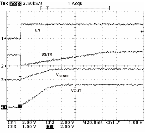
At power up, the TPS57060-Q1 device does not start switching until the slow start pin is discharged to less than 40 mV to ensure a proper power up, see Figure 30.
Also, during normal operation, the TPS57060-Q1 device stops switching and the SS/TR must be discharged to 40 mV, when the VIN UVLO is exceeded, EN pin pulled below 1.25 V, or a thermal shutdown event occurs.
The VSENSE voltage will follow the SS/TR pin voltage with a 45-mV offset up to 85% of the internal voltage reference. When the SS/TR voltage is greater than 85% on the internal reference voltage the offset increases as the effective system reference transitions from the SS/TR voltage to the internal voltage reference (see Figure 23). The SS/TR voltage will ramp linearly until clamped at 1.7 V.
 Figure 30. Operation of SS/TR Pin When Starting