ZHCSE52B September   2015  – May 2019 TPS57140-EP

PRODUCTION DATA.  

  1. 特性
  2. 应用范围
  3. 说明
    1.     Device Images
      1.      简化原理图
      2.      效率与负载电流间的关系
  4. 修订历史记录
  5. Pin Configuration and Functions
    1.     Pin Functions
  6. Specifications
    1. 6.1 Absolute Maximum Ratings
    2. 6.2 ESD Ratings
    3. 6.3 Recommended Operating Conditions
    4. 6.4 Thermal Information
    5. 6.5 Electrical Characteristics
    6. 6.6 Typical Characteristics
  7. Detailed Description
    1. 7.1 Overview
    2. 7.2 Functional Block Diagram
    3. 7.3 Feature Description
      1. 7.3.1  Fixed Frequency PWM Control
      2. 7.3.2  Slope-Compensation Output Current
      3. 7.3.3  Bootstrap Voltage (Boot)
      4. 7.3.4  Low-Dropout Operation
      5. 7.3.5  Error Amplifier
      6. 7.3.6  Voltage Reference
      7. 7.3.7  Adjusting the Output Voltage
      8. 7.3.8  Enable and Adjusting UVLO
      9. 7.3.9  Slow-Start or Tracking Pin (SS/TR)
      10. 7.3.10 Overload Recovery Circuit
      11. 7.3.11 Constant Switching Frequency and Timing Resistor (RT/CLK Pin)
      12. 7.3.12 Overcurrent Protection and Frequency Shift
      13. 7.3.13 Selecting the Switching Frequency
      14. 7.3.14 How to Interface to RT/CLK Pin
      15. 7.3.15 Power Good (PWRGD Pin)
      16. 7.3.16 Overvoltage Transient Protection (OVTP)
      17. 7.3.17 Thermal Shutdown
      18. 7.3.18 Small-Signal Model for Loop Response
      19. 7.3.19 Simple Small-Signal Model for Peak-Current-Mode Control
      20. 7.3.20 Small-Signal Model for Frequency Compensation
    4. 7.4 Device Functional Modes
      1. 7.4.1 Sequencing
      2. 7.4.2 Pulse-Skip Eco-mode Control Scheme
  8. Application and Implementation
    1. 8.1 Application Information
    2. 8.2 Typical Application
      1. 8.2.1 Design Requirements
      2. 8.2.2 Detailed Design Procedure
        1. 8.2.2.1  Selecting the Switching Frequency
        2. 8.2.2.2  Output Inductor Selection (LO)
        3. 8.2.2.3  Output Capacitor
        4. 8.2.2.4  Catch Diode
        5. 8.2.2.5  Input Capacitor
        6. 8.2.2.6  Slow-Start Capacitor
        7. 8.2.2.7  Bootstrap Capacitor Selection
        8. 8.2.2.8  UVLO Set Point
        9. 8.2.2.9  Output Voltage and Feedback Resistors Selection
        10. 8.2.2.10 Compensation
      3. 8.2.3 Application Curves
  9. Power Supply Recommendations
  10. 10Layout
    1. 10.1 Layout Guidelines
    2. 10.2 Layout Example
    3. 10.3 Power-Dissipation Estimate
  11. 11器件和文档支持
    1. 11.1 接收文档更新通知
    2. 11.2 社区资源
    3. 11.3 商标
    4. 11.4 静电放电警告
    5. 11.5 Glossary
  12. 12机械、封装和可订购信息

封装选项

机械数据 (封装 | 引脚)
散热焊盘机械数据 (封装 | 引脚)
订购信息

Typical Characteristics
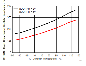
TPS57140-EP D001_SLVSD01.gif
Figure 2. On Resistance vs Junction Temperature
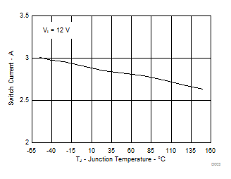
TPS57140-EP D003_SLVSD01.gif
Figure 4. Switch Current Limit vs Junction Temperature
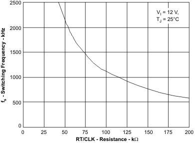
TPS57140-EP fs_rt_clk_lvs795.gif
Figure 6. Switching Frequency vs RT/CLK Resistance, High-Frequency Range
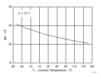
TPS57140-EP D005_SLVSD01.gif
Figure 8. EA Transconductance During Slow Start vs Junction Temperature
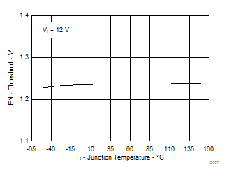
TPS57140-EP D007_SLVSD01.gif
Figure 10. EN Pin Voltage vs Junction Temperature
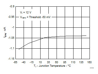
TPS57140-EP D009_SLVSD01.gif
Figure 12. EN Pin Current vs Junction Temperature
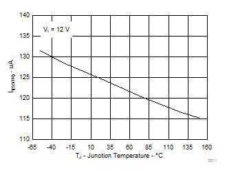
TPS57140-EP D011_SLVSD01.gif
Figure 14. SS/TR Discharge Current vs Junction Temperature
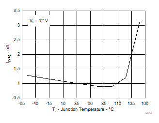
TPS57140-EP D012_SLVSD01.gif
Figure 16. Shutdown Supply Current vs Junction Temperature
TPS57140-EP D013_SLVSD01.gif
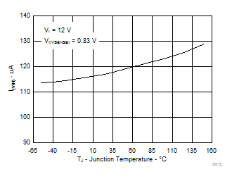
Figure 18. VIN Supply Current vs Junction Temperature
TPS57140-EP D014_SLVSD01.gif
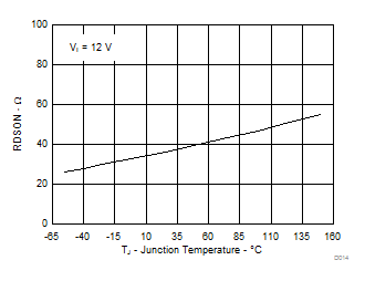
Figure 20. PWRGD On Resistance vs Junction Temperature
TPS57140-EP D016_SLVSD01.gif
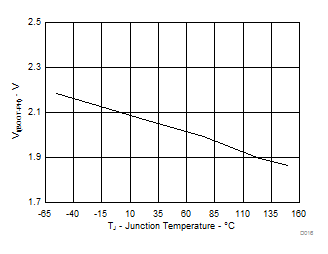
Figure 22. BOOT-PH UVLO vs Junction Temperature
TPS57140-EP offset_vs_lvs795.gif
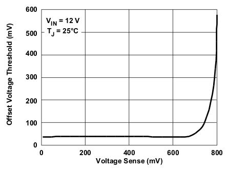
Figure 24. SS/TR to VSENSE Offset vs VSENSE
TPS57140-EP D002_SLVSD01.gif
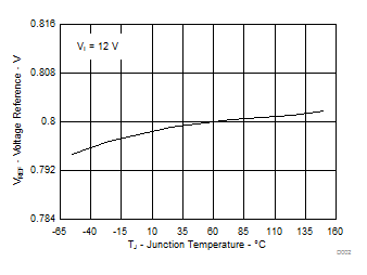
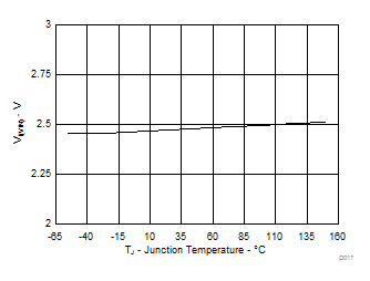
Figure 3. Voltage Reference vs Junction Temperature
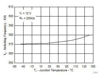
TPS57140-EP D004_SLVSD01.gif
Figure 5. Switching Frequency vs Junction Temperature
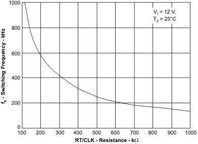
TPS57140-EP fs_rt_clk2_lvs795.gif
Figure 7. Switching Frequency vs RT/CLK Resistance, Low-Frequency Range
TPS57140-EP D006_SLVSD01.gif
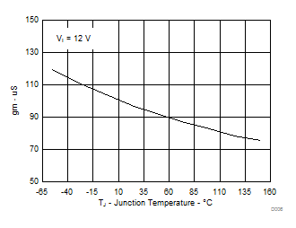
Figure 9. EA Transconductance vs Junction Temperature
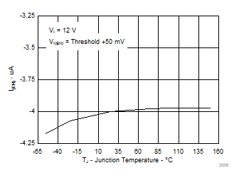
TPS57140-EP D008_SLVSD01.gif
Figure 11. EN Pin Current vs Junction Temperature
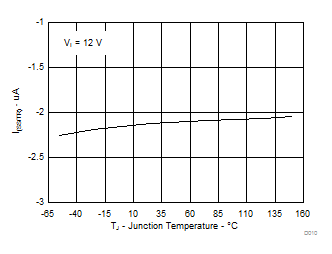
TPS57140-EP D010_SLVSD01.gif
Figure 13. SS/TR Charge Current vs Junction Temperature
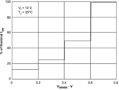
TPS57140-EP fs_vsense_lvs795.gif
Figure 15. Switching Frequency vs VSENSE
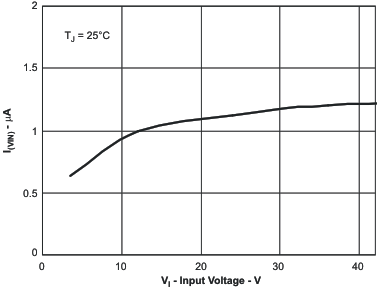
TPS57140-EP icc_vi_lvs795.gif
Figure 17. Shutdown Supply Current vs Input Voltage (VIN)
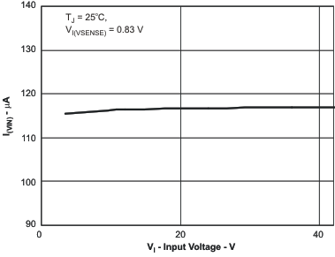
TPS57140-EP icc_vi2_lvs795.gif
Figure 19. VIN Supply Current vs Input Voltage
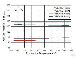
TPS57140-EP D015_SLVSD01.gif
Figure 21. PWRGD Threshold vs Junction Temperature
TPS57140-EP D017_SLVSD01.gif
Figure 23. Input Voltage (UVLO) vs Junction Temperature
TPS57140-EP D018_SLVSD01.gif
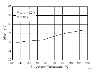
Figure 25. SS/TR to VSENSE Offset vs Temperature