ZHCSE52B September 2015 – May 2019 TPS57140-EP
PRODUCTION DATA.
- 1 特性
- 2 应用范围
- 3 说明
- 4 修订历史记录
- 5 Pin Configuration and Functions
- 6 Specifications
-
7 Detailed Description
- 7.1 Overview
- 7.2 Functional Block Diagram
- 7.3
Feature Description
- 7.3.1 Fixed Frequency PWM Control
- 7.3.2 Slope-Compensation Output Current
- 7.3.3 Bootstrap Voltage (Boot)
- 7.3.4 Low-Dropout Operation
- 7.3.5 Error Amplifier
- 7.3.6 Voltage Reference
- 7.3.7 Adjusting the Output Voltage
- 7.3.8 Enable and Adjusting UVLO
- 7.3.9 Slow-Start or Tracking Pin (SS/TR)
- 7.3.10 Overload Recovery Circuit
- 7.3.11 Constant Switching Frequency and Timing Resistor (RT/CLK Pin)
- 7.3.12 Overcurrent Protection and Frequency Shift
- 7.3.13 Selecting the Switching Frequency
- 7.3.14 How to Interface to RT/CLK Pin
- 7.3.15 Power Good (PWRGD Pin)
- 7.3.16 Overvoltage Transient Protection (OVTP)
- 7.3.17 Thermal Shutdown
- 7.3.18 Small-Signal Model for Loop Response
- 7.3.19 Simple Small-Signal Model for Peak-Current-Mode Control
- 7.3.20 Small-Signal Model for Frequency Compensation
- 7.4 Device Functional Modes
-
8 Application and Implementation
- 8.1 Application Information
- 8.2
Typical Application
- 8.2.1 Design Requirements
- 8.2.2
Detailed Design Procedure
- 8.2.2.1 Selecting the Switching Frequency
- 8.2.2.2 Output Inductor Selection (LO)
- 8.2.2.3 Output Capacitor
- 8.2.2.4 Catch Diode
- 8.2.2.5 Input Capacitor
- 8.2.2.6 Slow-Start Capacitor
- 8.2.2.7 Bootstrap Capacitor Selection
- 8.2.2.8 UVLO Set Point
- 8.2.2.9 Output Voltage and Feedback Resistors Selection
- 8.2.2.10 Compensation
- 8.2.3 Application Curves
- 9 Power Supply Recommendations
- 10Layout
- 11器件和文档支持
- 12机械、封装和可订购信息
7.3.8 Enable and Adjusting UVLO
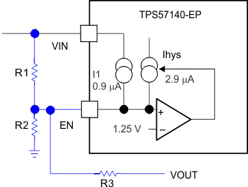
The VIN pin voltage falling below 2.5 V disables the TPS57140-EP. If an application requires a higher UVLO, use the EN pin as shown in Figure 28 to adjust the input-voltage UVLO by using two external resistors. Though it is not necessary to use the UVLO adjust resistors, for operation, TI highly recommends providing consistent power-up behavior. The EN pin has an internal pullup current source, I1, of 0.9 μA that provides the default condition of the TPS57140-EP operating when the EN pin floats. When the EN pin voltage exceeds 1.25 V, an additional 2.9 μA of hysteresis, Ihys, is added. This additional current facilitates input-voltage hysteresis. Use Equation 2 to set the external hysteresis for the input voltage. Use Equation 3 to set the input start voltage.
 Figure 28. Adjustable UVLO

Figure 29 shows another technique to add input-voltage hysteresis. The designer can use this method if the resistance values are high from the previous method and there is a need for a wider voltage hysteresis. Resistor R3 sources additional hysteresis current into the EN pin.
 Figure 29. Adding Additional Hysteresis

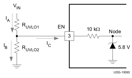
Do not place a low-impedance voltage source with >5 V directly on the EN pin. Do not place a capacitor directly on the EN pin if VEN > 5 V when using a voltage divider to adjust the start and stop voltage. The node voltage (see Figure 30) must remain ≤5.8 V. The Zener diode can sink up to 100 μA. The EN pin voltage can be >5 V if the VIN voltage source has a high impedance and does not source more than 100 μA into the EN pin.
 Figure 30. Node Voltage