SLVS279D March 2000 – August 2015 TPS61000 , TPS61002 , TPS61005 , TPS61006 , TPS61007
PRODUCTION DATA.
- 1 Features
- 2 Applications
- 3 Description
- 4 Revision History
- 5 Available Options
- 6 Pin Configuration and Functions
- 7 Specifications
- 8 Parameter Measurement Information
- 9 Detailed Description
- 10Application and Implementation
- 11Power Supply Recommendations
- 12Layout
- 13Device and Documentation Support
- 14Mechanical, Packaging, and Orderable Information
请参考 PDF 数据表获取器件具体的封装图。
机械数据 (封装 | 引脚)
- DGS|10
散热焊盘机械数据 (封装 | 引脚)
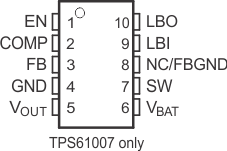
6 Pin Configuration and Functions
DGS Package
10-Pin VSSOP
Top View

Pin Functions
| PIN | I/O | DESCRIPTION | |
|---|---|---|---|
| NAME | NO. | ||
| COMP | 2 | — | Compensation of error amplifier. Connect R-C-C network to set frequency response of control loop. See the Application section for more details. |
| EN | 1 | I | Chip-enable input. The converter is switched on if EN is set high, and is switched off when EN is connected to ground (shutdown mode). |
| FB | 3 | I | Feedback input for adjustable output voltage (TPS61000 only). The output voltage is programmed depending on the values of resistors R1 and R2. For the fixed output voltage versions (TPS61000, TPS61002, TPS61003, TPS61004, TPS61005, TPS61006), leave the FB pin unconnected. |
| NC/FBGND | 8 | — | Not connected (TPS61000, TPS61002, TPS61003, TPS61004, TPS61005, TPS61006). A ground pin for the feedback resistor divider for the TPS61007 only. |
| GND | 4 | — | Ground |
| LBI | 9 | I | Low-battery detector input. A low-battery signal is generated at the LBO pin when the voltage on LBI drops below the threshold of 500 mV. Connect LBI to GND or VBAT if the low-battery detector function is not used. Do not leave this pin floating. |
| LBO | 10 | O | Open-drain low-battery detector output. This pin is pulled low if the voltage on LBI drops below the threshold of 500 mV. A pullup resistor should be connected between LBO and VOUT. |
| SW | 7 | I | Switch input pin. The node between inductor and anode of the rectifier diode is connected to this pin. |
| VBAT | 6 | I | Supply pin |
| VOUT | 5 | O | Output voltage. For the fixed output voltage versions, the integrated resistive divider is connected to this pin. |