SLVS314F SEPTEMBER 2000 – August 2015 TPS61010 , TPS61012 , TPS61013 , TPS61014 , TPS61015 , TPS61016
PRODUCTION DATA.
- 1 Features
- 2 Applications
- 3 Description
- 4 Revision History
- 5 Device Comparison Table
- 6 Pin Configuration and Functions
- 7 Specifications
- 8 Parameter Measurement Information
- 9 Detailed Description
-
10Application and Implementation
- 10.1 Application Information
- 10.2
Typical Applications
- 10.2.1 1.8-mm Maximum Height Power Supply With Single Battery Cell Input Using Low Profile Components
- 10.2.2 250-mA Power Supply With Two Battery Cell Input
- 10.2.3 Dual Output Voltage Power Supply for DSPs
- 10.2.4 Power Supply With Auxiliary Positive Output Voltage
- 10.2.5 Power Supply With Auxiliary Negative Output Voltage
- 10.2.6 TPS6101x EVM Circuit Diagram
- 11Power Supply Recommendations
- 12Layout
- 13Device and Documentation Support
- 14Mechanical, Packaging, and Orderable Information
6 Pin Configuration and Functions
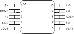
DGS PACKAGE
10 PINS
(TOP VIEW)

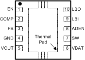
DRC PACKAGE
10 PINS
(TOP VIEW)

Pin Functions
| PIN | I/O | DESCRIPTION | ||
|---|---|---|---|---|
| NAME | DRG NO. |
DRC NO. |
||
| ADEN | 8 | 8 | I | Autodischarge output. The autodischarge function is enabled if this pin is connected to VBAT, it is disabled if ADEN is tied to GND. |
| COMP | 2 | 2 | I | Compensation of error amplifier. Connect an R/C/C network to set frequency response of control loop. |
| EN | 1 | 1 | I | Chip-enable input. The converter is switched on if this pin is set high, it is switched off if this pin is connected to GND. |
| FB | 3 | 3 | I | Feedback input for adjustable output voltage version TPS61010. Output voltage is programmed depending on the output voltage divider connected there. For the fixed output voltage versions, leave FB-pin unconnected. |
| GND | 4 | 4 | Ground | |
| LBI | 9 | 9 | I | Low-battery detector input. A low battery warning is generated at LBO when the voltage on LBI drops below the threshold of 500 mV. Connect LBI to GND or VBAT if the low-battery detector function is not used. Do not leave this pin floating. |
| LBO | 10 | 10 | O | Open-drain low-battery detector output. This pin is pulled low if the voltage on LBI drops below the threshold of 500 mV. A pullup resistor must be connected between LBO and VOUT. |
| SW | 7 | 7 | I | Switch input pin. The inductor is connected to this pin. |
| VBAT | 6 | 6 | I | Supply pin |
| VOUT | 5 | 5 | O | Output voltage. Internal resistor divider sets regulated output voltage in fixed output voltage versions. |