SLVS314F SEPTEMBER 2000 – August 2015 TPS61010 , TPS61012 , TPS61013 , TPS61014 , TPS61015 , TPS61016
PRODUCTION DATA.
- 1 Features
- 2 Applications
- 3 Description
- 4 Revision History
- 5 Device Comparison Table
- 6 Pin Configuration and Functions
- 7 Specifications
- 8 Parameter Measurement Information
- 9 Detailed Description
-
10Application and Implementation
- 10.1 Application Information
- 10.2
Typical Applications
- 10.2.1 1.8-mm Maximum Height Power Supply With Single Battery Cell Input Using Low Profile Components
- 10.2.2 250-mA Power Supply With Two Battery Cell Input
- 10.2.3 Dual Output Voltage Power Supply for DSPs
- 10.2.4 Power Supply With Auxiliary Positive Output Voltage
- 10.2.5 Power Supply With Auxiliary Negative Output Voltage
- 10.2.6 TPS6101x EVM Circuit Diagram
- 11Power Supply Recommendations
- 12Layout
- 13Device and Documentation Support
- 14Mechanical, Packaging, and Orderable Information
7 Specifications
7.1 Absolute Maximum Ratings
over operating free-air temperature range (unless otherwise noted)(1)| MIN | MAX | UNIT | ||
|---|---|---|---|---|
| Input voltage | VBAT, VOUT, EN, LBI, FB, ADEN | –0.3 | 3.6 | V |
| SW | –0.3 | 7 | V | |
| Voltage | LBO, COMP | –0.3 | 3.6 | V |
| Operating free-air temperature range, TA | –40 | 85 | °C | |
| Maximum junction temperature, TJ | 150 | °C | ||
| Storage temperature range, Tstg | –65 | 150 | °C | |
(1) Stresses beyond those listed under Absolute Maximum Ratings may cause permanent damage to the device. These are stress ratings only, and functional operation of the device at these or any other conditions beyond those indicated under Recommended Operating Conditions is not implied. Exposure to absolute-maximum-rated conditions for extended periods may affect device reliability.
7.2 ESD Ratings
| VALUEMAX | UNIT | |||
|---|---|---|---|---|
| V(ESD) | Electrostatic discharge | Human body model (HBM), per ANSI/ESDA/JEDEC JS-001, all pins(1) | ±2000 | V |
| Charged device model (CDM), per JEDEC specification JESD22-C101, all pins(2) | ±1000 | |||
(1) JEDEC document JEP155 states that 500-V HBM allows safe manufacturing with a standard ESD control process.
(2) JEDEC document JEP157 states that 250-V CDM allows safe manufacturing with a standard ESD control process.
7.3 Recommended Operating Conditions
| MIN | NOM | MAX | UNIT | ||
|---|---|---|---|---|---|
| VI | Supply voltage at VBAT | 0.8 | VOUT | V | |
| IO | Maximum output current at VIN = 1.2 V | 100 | mA | ||
| IO | Maximum output current at VIN = 2.4 V | 200 | mA | ||
| L1 | Inductor | 10 | 33 | µH | |
| CI | Input capacitor | 10 | µF | ||
| Co | Output capacitor | 10 | 22 | 47 | µF |
| TJ | Operating virtual junction temperature | –40 | 125 | °C | |
7.4 Thermal Information
| THERMAL METRIC(1) | TPS6101x | TPS61010 | UNIT | |
|---|---|---|---|---|
| DGS | DRC | |||
| 10 PINS | ||||
| RθJA | Junction-to-ambient thermal resistance | 161.8 | 43.1 | °C/W |
| RθJC(top) | Junction-to-case (top) thermal resistance | 36.3 | 67.4 | |
| RθJB | Junction-to-board thermal resistance | 82.7 | 18.1 | |
| ψJT | Junction-to-top characterization parameter | 1.3 | 1.6 | |
| ψJB | Junction-to-board characterization parameter | 81.1 | 18.2 | |
| RθJC(bot) | Junction-to-case (bottom) thermal resistance | N/A | 5.2 | |
(1) For more information about traditional and new thermal metrics, see the IC Package Thermal Metrics application report, SPRA953.
7.5 Electrical Characteristics
over recommended operating free-air temperature range, VBAT = 1.2 V, EN = VBAT (unless otherwise noted)| PARAMETER | TEST CONDITIONS | MIN | TYP | MAX | UNIT | ||
|---|---|---|---|---|---|---|---|
| VI | Minimum input voltage for start-up | RL = 33 Ω | 0.85 | 0.9 | V | ||
| RL = 3 kΩ, TA = 25 °C | 0.8 | ||||||
| Input voltage once started | IO = 100 mA | 0.8 | |||||
| VO | Programmable output voltage range |
TPS61010, IOUT = 100 mA | 1.5 | 3.3 | V | ||
| Output voltage | TPS61011, 0.8 V < VI < VO, IO = 0 to 100 mA | 1.45 | 1.5 | 1.55 | V | ||
| TPS61012, 0.8 V < VI < VO, IO = 0 to 100 mA | 1.74 | 1.8 | 1.86 | ||||
| TPS61013, 0.8 V < VI < VO, IO = 0 to 100 mA | 2.42 | 2.5 | 2.58 | V | |||
| TPS61013, 1.6 V < VI < VO, IO = 0 to 200 mA | 2.42 | 2.5 | 2.58 | V | |||
| TPS61014, 0.8 V < VI < VO, IO = 0 to 100 mA | 2.72 | 2.8 | 2.88 | V | |||
| TPS61014, 1.6 V < VI < VO, IO = 0 to 200 mA | 2.72 | 2.8 | 2.88 | V | |||
| TPS61015, 0.8 V < VI < VO, IO = 0 to 100 mA | 2.9 | 3.0 | 3.1 | V | |||
| TPS61015, 1.6 V < VI < VO, IO = 0 to 200 mA | 2.9 | 3.0 | 3.1 | V | |||
| TPS61016, 0.8 V < VI < VO, IO = 0 to 100 mA | 3.2 | 3.3 | 3.4 | V | |||
| TPS61016, 1.6 V < VI < VO, IO = 0 to 200 mA | 3.2 | 3.3 | 3.4 | V | |||
| IO | Maximum continuous output current | VI > 0.8 V | 100 | mA | |||
| VI > 1.8 V | 250 | ||||||
| I(SW) | Switch current limit | TPS61011, once started | 0.39 | 0.48 | A | ||
| TPS61012, once started | 0.54 | 0.56 | |||||
| TPS61013, once started | 0.85 | 0.93 | |||||
| TPS61014, once started | 0.95 | 1.01 | |||||
| TPS61015, once started | 1 | 1.06 | |||||
| TPS61016, once started | 1.07 | 1.13 | |||||
| V(FB) | Feedback voltage | 480 | 500 | 520 | mV | ||
| f | Oscillator frequency | 420 | 500 | 780 | kHz | ||
| D | Maximum duty cycle | 85% | |||||
| rDS(on) | NMOS switch on-resistance | VO = 1.5 V | 0.37 | 0.51 | Ω | ||
| PMOS switch on-resistance | 0.45 | 0.54 | |||||
| rDS(on) | NMOS switch on-resistance | VO = 3.3 V | 0.2 | 0.37 | Ω | ||
| PMOS switch on-resistance | 0.3 | 0.45 | |||||
| Line regulation (1) | VI = 1.2 V to 1.4 V, IO = 100 mA | 0.3 | %/V | ||||
| Load regulation (1) | VI = 1.2 V; IO = 50 mA to 100 mA | 0.1 | |||||
| Autodischarge switch resistance |
300 | 400 | Ω | ||||
| Residual output voltage after autodischarge | ADEN = VBAT; EN = GND | 0.4 | V | ||||
| VIL | LBI voltage threshold (2) | V(LBI) voltage decreasing | 480 | 500 | 520 | mV | |
| LBI input hysteresis | 10 | mv | |||||
| LBI input current | 0.01 | 0.03 | |||||
| VOL | LBO output low voltage | V(LBI) = 0 V, VO = 3.3 V, I(OL) = 10 µA | 0.04 | 0.2 | V | ||
| LBO output leakage current | V(LBI) = 650 mV, V(LBO) = VO | 0.03 | µA | ||||
| I(FB) | FB input bias current (TPS61010 only) | V(FB) = 500 mV | 0.01 | 0.03 | |||
| VIL | EN and ADEN input low voltage | 0.8 V < VBAT < 3.3 V | 0.2 × VBAT | V | |||
| VIH | EN and ADEN input high voltage | 0.8 V < VBAT < 3.3 V | 0.8 ×VBAT | V | |||
| EN and ADEN input current | EN and ADEN = GND or VBAT | 0.01 | 0.03 | µA | |||
| Iq | Quiescent current into pins VBAT/SW and VOUT | IL = 0 mA, VEN = VI | VBAT/SW | 31 | 46 | µA | |
| VO | 5 | 8 | |||||
| Ioff | Shutdown current from power source | VEN = 0 V, ADEN = VBAT, TA= 25°C | 1 | 3 | µA | ||
(1) Line and load regulation is measured as a percentage deviation from the nominal value (i.e., as percentage deviation from the nominal output voltage). For line regulation, x %/V stands for ±x% change of the nominal output voltage per 1-V change on the input/supply voltage. For load regulation, y% stands for ±y% change of the nominal output voltage per the specified current change.
(2) For proper operation the voltage at LBI may not exceed the voltage at VBAT.
7.6 Typical Characteristics
7.6.1 Table of Graphs
| FIGURE | ||
|---|---|---|
| Maximum output current | vs Input voltage for VO = 2.5 V, 3.3 V | Figure 1 |
| vs Input voltage for VO = 1.5 V, 1.8 V | Figure 2 | |
| Efficiency | vs Output current for VI = 1.2 VVO = 1.5 V, L1 = Sumida CDR74 - 10 µH | Figure 3 |
| vs Output current for VI = 1.2 VVO = 2.5 V, L1 = Sumida CDR74 - 10 µH | Figure 4 | |
| vs Output current for VIN = 1.2 VVO = 3.3 V, L1 = Sumida CDR74 - 10 µH | Figure 5 | |
| vs Output current for VI = 2.4 VVO = 3.3 V, L1 = Sumida CDR74 - 10 µH | Figure 6 | |
| vs Input voltage for IO = 10 mA, IO = 100 mA, IO = 200 mAVO = 3.3 V, L1 = Sumida CDR74 - 10 µH | Figure 7 | |
| TPS61016, VBAT = 1.2 V, IO = 100 mA | Figure 8 | |
| Sumida CDRH6D38 - 10 µH | ||
| Sumida CDRH5D18 - 10 µH | ||
| Sumida CDRH74 - 10 µH | ||
| Sumida CDRH74B - 10 µH | ||
| Coilcraft DS 1608C - 10 µH | ||
| Coilcraft DO 1608C - 10 µH | ||
| Coilcraft DO 3308P - 10 µH | ||
| Coilcraft DS 3316 - 10 µH | ||
| Coiltronics UP1B - 10 µH | ||
| Coiltronics UP2B - 10 µH | ||
| Murata LQS66C - 10 µH | ||
| Murata LQN6C - 10 µH | ||
| TDK SLF 7045 - 10 µH | ||
| TDK SLF 7032 - 10 µH | ||
| Output voltage | vs Output current TPS61011 | Figure 9 |
| vs Output current TPS61013 | Figure 10 | |
| vs Output current TPS61016 | Figure 11 | |
| Minimum supply start-up voltage | vs Load resistance | Figure 12 |
| No-load supply current | vs Input voltage | Figure 13 |
| Shutdown supply current | vs Input voltage | Figure 14 |
| Switch current limit | vs Output voltage | Figure 15 |
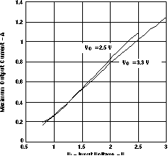
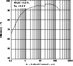 Figure 3. Efficiency vs Output Current
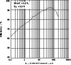 Figure 5. Efficiency vs Output Current
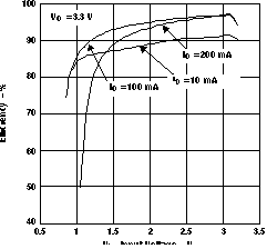 Figure 7. Efficiency vs Input Voltage
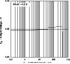 Figure 9. Output Voltage vs Output Current
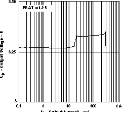 Figure 11. Output Voltage vs Output Current
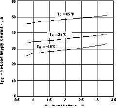 Figure 13. No-Load Supply Current vs Input Voltage
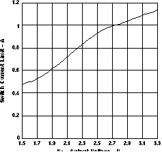 Figure 15. Switch Current Limit vs Output Voltage
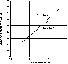
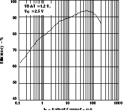 Figure 4. Efficiency vs Output Current
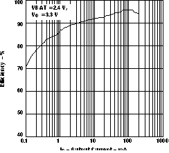 Figure 6. Efficiency vs Output Current
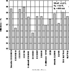 Figure 8. Efficiency vs Inductor Type
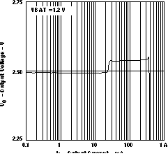 Figure 10. Output Voltage vs Output Current
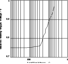 Figure 12. Minimum Start-Up Supply Voltage vs Load Resistance
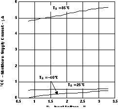 Figure 14. Shutdown Supply Current vs Input Voltage