ZHCSFA0 June 2016 TPS61021A
PRODUCTION DATA.
- 1 特性
- 2 应用
- 3 说明
- 4 修订历史记录
- 5 Pin Configuration and Functions
- 6 Specifications
- 7 Detailed Description
- 8 Application and Implementation
- 9 Power Supply Recommendations
- 10Layout
- 11器件和文档支持
- 12机械、封装和可订购信息
6 Specifications
6.1 Absolute Maximum Ratings
over operating free-air temperature range (unless otherwise noted)(1)| MIN | MAX | UNIT | |||
|---|---|---|---|---|---|
| Voltage range at terminals(2) | EN, FB | DC | –0.3 | 3.6 | V |
| VIN, SW, VOUT | DC | –0.3 | 4.6 | V | |
| 10% duty cycle | –0.3 | 4.8 | V | ||
| Operating junction temperature, TJ | –40 | 150 | °C | ||
| Storage temperature, Tstg | –65 | 150 | °C | ||
(1) Stresses beyond those listed under Absolute Maximum Ratings may cause permanent damage to the device. These are stress ratings only, which do not imply functional operation of the device at these or any other conditions beyond those indicated under Recommended Operating Conditions. Exposure to absolute-maximum-rated conditions for extended periods may affect device reliability.
(2) All voltage values are with respect to network ground terminal.
6.2 ESD Ratings
| VALUE | UNIT | |||
|---|---|---|---|---|
| V(ESD) | Electrostatic discharge | Human-body model (HBM), per ANSI/ESDA/JEDEC JS-001(1) | ±2000 | V |
| Charged-device model (CDM), per JEDEC specification JESD22-C101(2) | ±500 | |||
(1) JEDEC document JEP155 states that 500-V HBM allows safe manufacturing with a standard ESD control process. Manufacturing with less than 500-V HBM is possible with the necessary precautions. Pins listed as ±2000 V may actually have higher performance.
(2) JEDEC document JEP157 states that 250-V CDM allows safe manufacturing with a standard ESD control process. Manufacturing with less than 250-V CDM is possible with the necessary precautions. Pins listed as ±500 V may actually have higher performance.
6.3 Recommended Operating Conditions
over operating free-air temperature range (unless otherwise noted)| MIN | NOM | MAX | UNIT | |||
|---|---|---|---|---|---|---|
| VIN | Input voltage range | 0.5 | 4.4 | V | ||
| VOUT | Output voltage setting range | 1.8 | 4.0 | V | ||
| L | Effective inductance range | 0.2 | 0.47 | 1.3 | µH | |
| CIN | Effective input capacitance range | 1.0 | 4.7 | µF | ||
| COUT | Effective output capacitance range | IOUT ≤ 0.3 A | 3.0 | 10 | 200 | µF |
| IOUT > 0.3 A | 10 | 20 | 200 | µF | ||
| TJ | Operating junction temperature | –40 | 125 | °C | ||
6.4 Thermal Information
| THERMAL METRIC(1) | TPS61021A | UNIT | |
|---|---|---|---|
| DSG (WSON) | |||
| 8 PINS | |||
| RθJA | Junction-to-ambient thermal resistance | 71.1 | °C/W |
| RθJC(top) | Junction-to-case (top) thermal resistance | 95.2 | °C/W |
| RθJB | Junction-to-board thermal resistance | 41.6 | °C/W |
| ψJT | Junction-to-top characterization parameter | 3.1 | °C/W |
| ψJB | Junction-to-board characterization parameter | 42.0 | °C/W |
| RθJC(bot) | Junction-to-case (bottom) thermal resistance | 13.0 | °C/W |
(1) For more information about traditional and new thermal metrics, see the Semiconductor and IC Package Thermal Metrics application report, SPRA953.
6.5 Electrical Characteristics
TJ = –40°C to 125°C, VIN = 2.4 V and VOUT = 3.3 V. Typical values are at TJ = 25°C (unless otherwise noted)| PARAMETER | TEST CONDITIONS | MIN | TYP | MAX | UNIT | |
|---|---|---|---|---|---|---|
| POWER SUPPLY | ||||||
| VIN | Input voltage range | 0.5 | 4.4 | V | ||
| VIN_UVLO | Under-voltage lockout threshold | VIN rising | 0.8 | 0.9 | V | |
| VIN falling | 0.28 | 0.4 | 0.5 | V | ||
| IQ | Quiescent current into VIN pin | IC enabled, No load, No switching VIN = 1.8 V to 3.6 V, VFB = VREF + 0.1 V, TJ up to 85°C | 3.0 | µA | ||
| Quiescent current into VOUT pin | IC enabled, No load, No switching VOUT = 1.8 V to 4.0 V, VFB = VREF + 0.1 V, TJ up to 85°C | 17 | 30 | µA | ||
| ISD | Shutdown current into VIN and SW pin | IC disabled, VIN = 1.8 V to 3.6 V, TJ up to 85°C | 0.5 | 3.0 | µA | |
| OUTPUT | ||||||
| VOUT | Output voltage setting range | 1.8 | 4.0 | V | ||
| VREF | Reference voltage at the FB pin | PWM mode | 775 | 795 | 815 | mV |
| PFM mode | 801 | mV | ||||
| VOVP | Output over-voltage protection threshold | VOUT rising | 4.15 | 4.35 | 4.60 | V |
| VOVP_HYS | Over-voltage protection hysteresis | 0.1 | V | |||
| IFB_LKG | Leakage current at FB pin | 20 | nA | |||
| ISW_LKG | Leakage current into SW pin | IC disabled, TJ up to 85°C | 3.0 | µA | ||
| IVOUT_LKG | Leakage current into VOUT pin | IC disabled, VOUT = 4.0 V, TJ up to 85°C | 1 | 2 | µA | |
| POWER SWITCH | ||||||
| RDS(on) | High-side MOSFET on resistance | VOUT = 3.3 V | 51 | mΩ | ||
| Low-side MOSFET on resistance | VOUT = 3.3 V | 58 | mΩ | |||
| fSW | Switching frequency | VIN = 2.4 V, VOUT = 3.3 V, PWM mode | 2.0 | MHZ | ||
| tOFF_min | Minimum off time | 80 | 120 | ns | ||
| ILIM_SW | Valley current limit | VIN = 2.4 V, VOUT = 3.3 V | 3.0 | 4.3 | A | |
| LOGIC INTERFACE | ||||||
| VEN_H | EN Logic high threshold | VIN > 1.2 V | 0.84 | V | ||
| VIN ≤ 1.2 V | 0.7 x VIN | |||||
| VEN_L | EN Logic Low threshold | VIN > 1.2 V | 0.36 | V | ||
| VIN ≤ 1.2 V | 0.3 x VIN | |||||
| PROTECTION | ||||||
| TSD | Thermal shutdown threshold | TJ rising | 150 | °C | ||
| TSD_HYS | Thermal shutdown hysteresis | TJ falling below TSD | 20 | °C | ||
6.6 Typical Characteristics
VIN = 2.4 V, VOUT = 3.3 V, TJ = 25°C, unless otherwise noted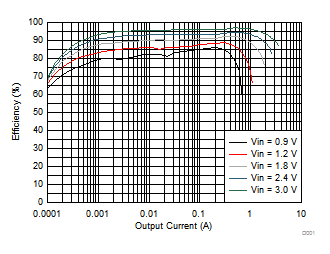
| VIN = 0.9 V, 1.2 V, 1.8 V, 2.4 V, 3.0 V, and VOUT = 3.3 V | ||
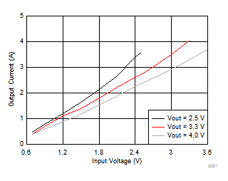
| VIN = 0.7 V to 3.6 V, VOUT = 2.5 V, 3.3 V, 4.0 V | ||

| VIN = 2.4 V, VOUT = 3.3 V, T = –40°C to 125°C | ||
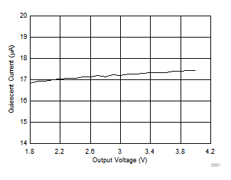
| VIN = 1.2 V, VOUT = 1.8 V to 4.0 V, No switching | ||

| VIN = 2.4 V, Into VIN and SW, T = –40°C to 85°C | ||
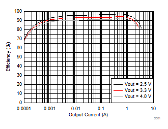
| VIN = 2.4 V, and VOUT = 2.5 V, 3.3 V, 4.0 V | ||

| VIN = 0.9 V, 1.6 V, 2.4 V, 3.0 V, and VOUT = 3.3 V | ||
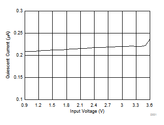
| VIN = 0.9 V to 3.6 V, VOUT = 4.0 V, No switching | ||

| VIN = 2.4 V, VOUT = 3.3 V, No switching, T = –40°C to 85°C | ||