ZHCSFA0 June 2016 TPS61021A
PRODUCTION DATA.
- 1 特性
- 2 应用
- 3 说明
- 4 修订历史记录
- 5 Pin Configuration and Functions
- 6 Specifications
- 7 Detailed Description
- 8 Application and Implementation
- 9 Power Supply Recommendations
- 10Layout
- 11器件和文档支持
- 12机械、封装和可订购信息
7 Detailed Description
7.1 Overview
The TPS61021A synchronous step-up converter is designed to operate from an input voltage supply range between 0.5 V and 4.4 V with 3-A valley switch current limit. The TPS61021A typically operates at a quasi-constant frequency pulse width modulation (PWM) at moderate to heavy load currents. The switching frequency is 2 MHz when the input voltage is above 1.5 V. The switching frequency reduces down to 1 MHz when the input voltage goes down from 1.5 V to 1 V. At light load currents, the TPS61021A converter operates in power-save mode with pulse frequency modulation (PFM). During PWM operation, the converter uses adaptive constant on-time valley current mode control scheme to achieve excellent line/load regulation and allows the use of a small inductor and ceramic capacitors. Internal loop compensation simplifies the design process while minimizing the number of external components.
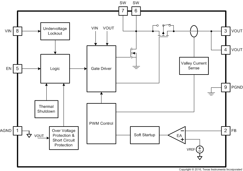
7.2 Functional Block Diagram

7.3 Feature Description
7.3.1 Under-Voltage Lockout
The TPS61021A has a built-in under-voltage lockout (UVLO) circuit to ensure the device working properly. When the input voltage is above the UVLO rising threshold of 0.9 V, the TPS61021A can be enabled to boost the output voltage. After the TPS61021A starts up and the output voltage is above 1.6 V, the TPS61021A can work with the input voltage as low as 0.5 V.
7.3.2 Enable and Soft Start
When the input voltage is above the under-voltage lockout (UVLO) rising threshold and the EN pin is pulled to logic high voltage, the TPS61021A is enabled and starts up. At the beginning, the switching frequency and current limit are internally controlled. The load capability is limited. After the output voltage is above 1.6 V, the peak current limit is determined by the output of an internal error amplifier which compares the feedback of the output voltage and the internal reference voltage. Because the output voltage is below the setting target, the peak current limit rises and thus the output voltage ramps quickly. The soft startup time varies with the different output capacitance and load condition. The typical startup time is around 200 μs for a 44-μF output capacitor with no load.
7.3.3 Switching Frequency
The TPS61021A switches at a quasi-constant 2-MHz frequency when the input voltage is above 1.5 V. When the input voltage declines from 1.5 V to 1 V, the switching frequency will be reduced gradually to 1-MHz to improve the efficiency and get higher boost ratio. When the input voltage is below 1 V, the switching frequency is fixed at a quasi-constant 1 MHz.
7.3.4 Current Limit Operation
The TPS61021A employs a valley current limit sensing scheme. Current limit detection occurs during the off-time by sensing of the voltage drop across the synchronous rectifier switch.
When the load current is increased such that the inductor current is above the current limit within the whole switching cycle time, the off-time is increased to allow the inductor current to decrease to this threshold before the next on-time begins (so called frequency fold-back mechanism). When the current limit is reached, the output voltage decreases during further load increase.
The maximum continuous output current (IOUT(CL)), before entering current limit (CL) operation, can be defined by Equation 1.

Where:
D is the duty cycle
ΔIL(P-P) is the inductor ripple current
The duty cycle can be estimated by Equation 2.

Where:
VOUT is the output voltage of the boost converter
VIN is the input voltage of the boost converter
η is the efficiency of the converter, use 90% for most applications
And the peak-to-peak inductor ripple current is calculated by Equation 3.

Where:
L is the inductance value of the inductor
fSW is the switching frequency
D is the duty cycle
VIN is the input voltage of the boost converter
7.3.5 Pass-Through Operation
When the input voltage is higher than the setting output voltage, the output voltage is higher than the target regulation voltage. When the output voltage is 101% of the setting target voltage, the TPS61021A stops switching and turns on the high side PMOS FET. The device works in pass-through mode. The output voltage is the input voltage minus the voltage drop across the dc resistance (DCR) of the inductor and the on-resistance (RDS(on)) of the PMOS FET. When the output voltage drops below the 98% of the setting target voltage as the input voltage declines or the load current increases, the TPS61021A resumes switching again to regulate the output voltage.
7.3.6 Over-Voltage Protection
The TPS61021A has an output over-voltage protection (OVP) to protect the device in case that the external feedback resistor divider is wrongly populated. When the output voltage is above 4.35 V typically, the device stops switching. Once the output voltage falls 0.1 V below the OVP threshold, the device resumes operating again. To prevent the high overshoot voltage during OVP when the FB pin voltage is too much lower than the internal reference voltage, the TPS61021A limits the valley swtich current to approximate 100 mA when the FB pin voltage is below 0.2 V and the output voltage is above 2.9V.
7.3.7 Output Short-to-Ground Protection
The TPS61021A starts to limit the output current when the output voltage is below 1.6 V. The lower the output voltage reaches, the smaller the output current is. When the output voltage is below 1 V, the output current is limited to approximate 100 mA. Once the short circuit is released, the TPS61021A goes through the soft startup again to output the regulated voltage.
7.3.8 Thermal Shutdown
The TPS61021A goes into thermal shutdown once the junction temperature exceeds 150°C. When the junction temperature drops below the thermal shutdown temperature threshold less the hysteresis, typically 130°C, the device starts operating again.
7.4 Device Functional Modes
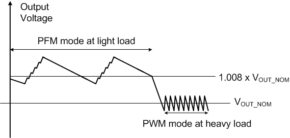
The TPS61021A has two switching operation modes, PWM mode in moderate to heavy load conditions and power save mode with pulse frequency modulation (PFM) in light load conditions.
7.4.1 PWM Mode
The TPS61021A uses a quasi-constant 2.0-MHz frequency pulse width modulation (PWM) at moderate to heavy load current. Based on the input voltage to output voltage ratio, a circuit predicts the required on-time. At the beginning of the switching cycle, the NMOS switching FET, shown in the functional block diagram, is turned on. The input voltage is applied across the inductor and the inductor current ramps up. In this phase, the output capacitor is discharged by the load current. When the on-time expires, the main switch NMOS FET is turned off, and the rectifier PMOS FET is turned on. The inductor transfers its stored energy to replenish the output capacitor and supply the load. The inductor current declines because the output voltage is higher than the input voltage. When the inductor current hits a value which the error amplifier outputs, the next switching cycle starts again.
The TPS61021A has a built-in compensation circuit that can accommodate a wide range of input voltage, output voltage, inductor value and output capacitor value for stable operation.
7.4.2 Power Save Mode
The TPS61021A integrates a power save mode with pulse frequency modulation (PFM) to improve efficiency at light load. When the load current decreases, the inductor valley current set by the output of the error amplifier declines to regulate the output voltage. When the inductor valley current hits the low limit of approximate 100 mA, the output voltage will exceed the setting voltage as the load current decreases further. When the FB voltage hits the PFM reference voltage, the TPS61021A goes into the power save mode. In the power save mode, when the FB voltage rises and hits the PFM reference voltage, the device continuous switching for several cycles because of the delay time of the internal comparator. Then it stops switching. The load is supplied by the output capacitor and the output voltage declines. When the FB voltage falls below the PFM reference voltage, after the delay time of the comparator, the device starts switching again to ramp up the output voltage.
 Figure 10. Output Voltage in PWM Mode and PFM Mode