ZHCSJB0D January 2019 – July 2021 TPS61022
PRODUCTION DATA
- 1 特性
- 2 应用
- 3 说明
- 4 Revision History
- 5 Pin Configuration and Functions
- 6 Specifications
- 7 Detailed Description
- 8 Application and Implementation
- 9 Power Supply Recommendations
- 10Layout
- 11Device and Documentation Support
- 12Mechanical, Packaging, and Orderable Information
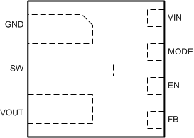
5 Pin Configuration and Functions
 Figure 5-1 7-Pin VQFN with Thermal Pad RWU
Package(Top View)
Figure 5-1 7-Pin VQFN with Thermal Pad RWU
Package(Top View)Table 5-1 Pin Functions
| PIN | I/O | DESCRIPTION | |
|---|---|---|---|
| NO. | NAME | ||
| 1 | GND | PWR | Ground pin of the IC. The GND pad of output capacitor must be close to the GND pin. Layout example is shown in Figure 10-1. |
| 2 | SW | PWR | The switch pin of the converter. It is connected to the drain of the internal low-side power MOSFET and the source of the internal high-side power MOSFET. |
| 3 | VOUT | PWR | Boost converter output. The VOUT pad of output capacitor must be close to the VOUT pin. Layout example is shown in Figure 10-1. |
| 4 | FB | I | Voltage feedback of adjustable output voltage. |
| 5 | EN | I | Enable logic input. Logic high voltage enables the device. Logic low voltage disables the device and turns it into shutdown mode. |
| 6 | MODE | I | Operation mode selection in the light load condition. When it is connected to logic high voltage, the device works in forced PWM mode. When it is connected to logic low voltage, the device works in auto PFM mode. |
| 7 | VIN | I | IC power supply input. |