ZHCSK97B September   2019  – August 2020 TPS61023

PRODUCTION DATA  

  1. 特性
  2. 应用
  3. 说明
  4. Revision History
  5. Pin Configuration and Functions
    1.     Pin Functions
  6. Specifications
    1. 6.1 Absolute Maximum Ratings
    2. 6.2 ESD Ratings
    3. 6.3 Recommended Operating Conditions
    4. 6.4 Thermal Information
    5. 6.5 Electrical Characteristics
    6. 6.6 Typical Characteristics
  7. Detailed Description
    1. 7.1 Overview
    2. 7.2 Functional Block Diagram
    3. 7.3 Feature Description
      1. 7.3.1 Undervoltage Lockout
      2. 7.3.2 Enable and Soft Start
      3. 7.3.3 Switching Frequency
      4. 7.3.4 Current Limit Operation
      5. 7.3.5 Pass-Through Operation
      6. 7.3.6 Overvoltage Protection
      7. 7.3.7 Output Short-to-Ground Protection
      8. 7.3.8 Thermal Shutdown
    4. 7.4 Device Functional Modes
      1. 7.4.1 PWM Mode
      2. 7.4.2 Power-Save Mode
  8. Application and Implementation
    1. 8.1 Application Information
    2. 8.2 Typical Application
      1. 8.2.1 Design Requirements
      2. 8.2.2 Detailed Design Procedure
        1. 8.2.2.1 Setting the Output Voltage
        2. 8.2.2.2 Inductor Selection
        3. 8.2.2.3 Output Capacitor Selection
        4. 8.2.2.4 Loop Stability, Feedforward Capacitor Selection
        5. 8.2.2.5 Input Capacitor Selection
      3. 8.2.3 Application Curves
  9. Power Supply Recommendations
  10. 10Layout
    1. 10.1 Layout Guidelines
    2. 10.2 Layout Example
    3. 10.3 Thermal Considerations
  11. 11Device and Documentation Support
    1. 11.1 Device Support
      1. 11.1.1 第三方米6体育平台手机版_好二三四免责声明
    2. 11.2 接收文档更新通知
    3. 11.3 支持资源
    4. 11.4 Trademarks
    5. 11.5 静电放电警告
    6. 11.6 术语表
  12. 12Mechanical, Packaging, and Orderable Information
    1. 12.1 Package Option Addendum
    2. 12.2 Tape and Reel Information

封装选项

机械数据 (封装 | 引脚)
散热焊盘机械数据 (封装 | 引脚)

Application Curves

GUID-DF5EA665-F698-44E7-BC81-DDB29CCA1987-low.gif
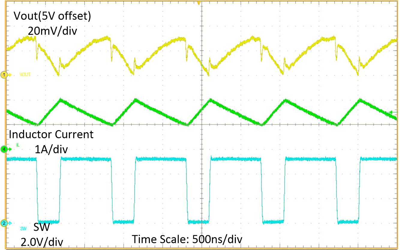
VIN = 3.6 V, VOUT = 5 V, IOUT = 1 A
Figure 8-3 Switching Waveform at Heavy Load
GUID-1E71DADF-C721-48CD-9171-37421CBEC6D7-low.gif
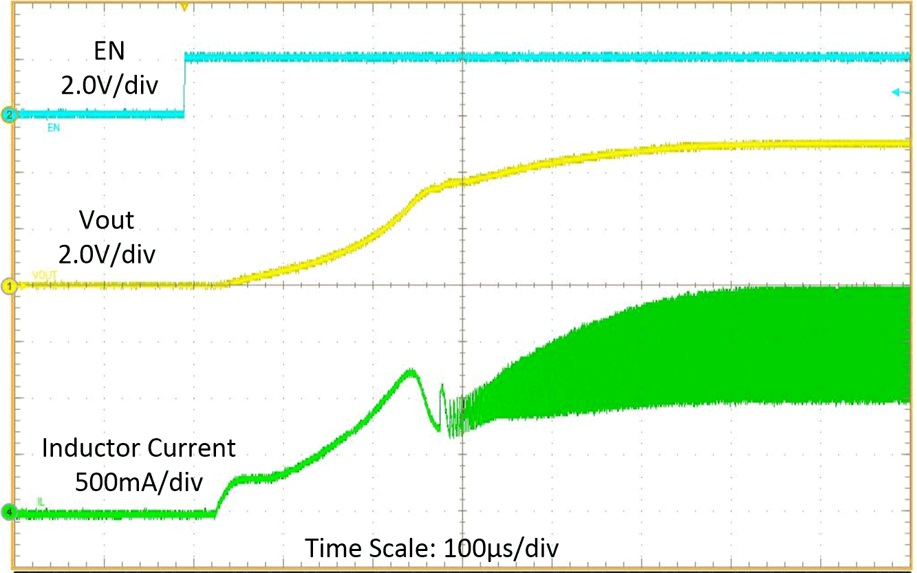
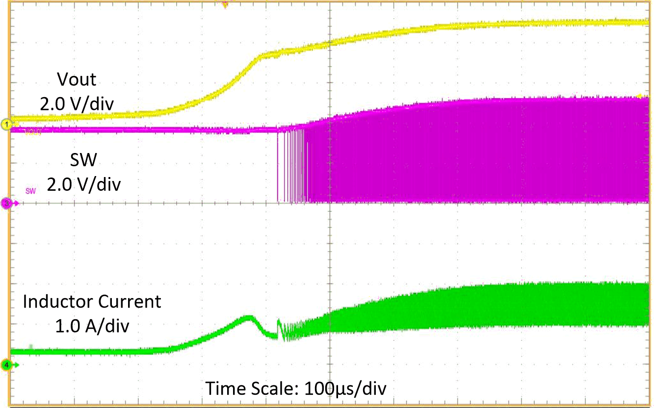
VIN = 3.6 V, VOUT = 5 V, 5-Ω resistance load
Figure 8-5 Start-up Waveform
GUID-0A5BD84F-8338-4718-8B59-29DEE4DFFFE5-low.gif
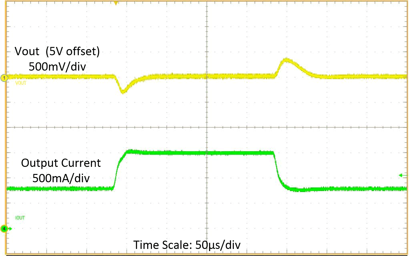
VIN = 3.6 V, VOUT = 5 V, IOUT = 800 mA to 1.5 A with 20-μs slew rate
Figure 8-7 Load Transient
GUID-79AF02D4-E62A-4925-898C-2D773549F73A-low.gif
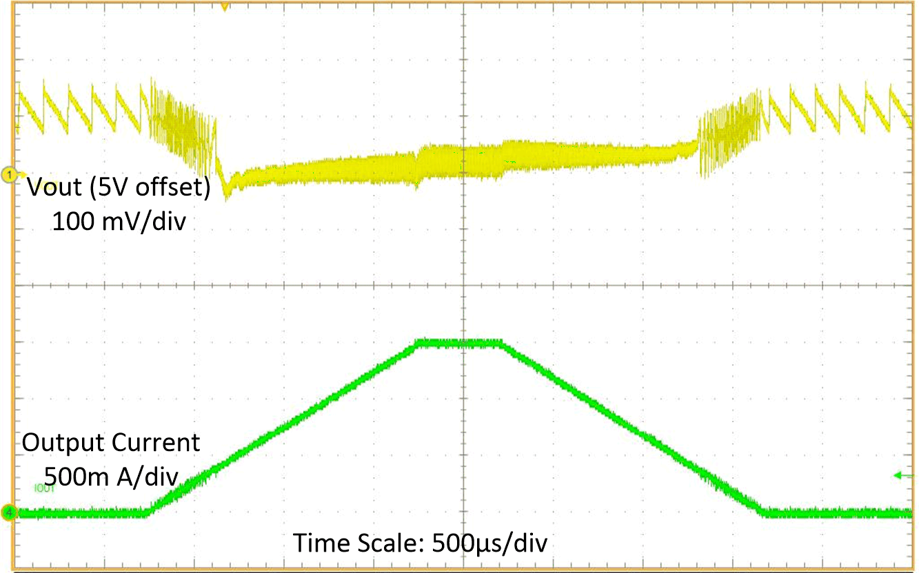
VIN = 3.6 V, VOUT = 5 V, IOUT = 0 A to 1.5 A Sweep
Figure 8-9 Load Sweep
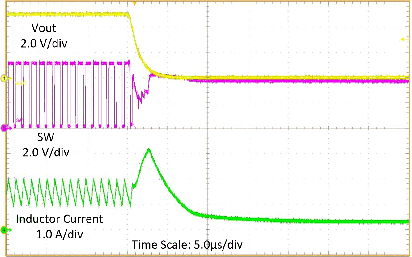
GUID-2F747BFD-C146-4A79-BD98-DBFD52960FE5-low.gif
VIN = 3.6 V, VOUT = 5 V, IOUT = 1 A
Figure 8-11 Output Short Protection (Entry)
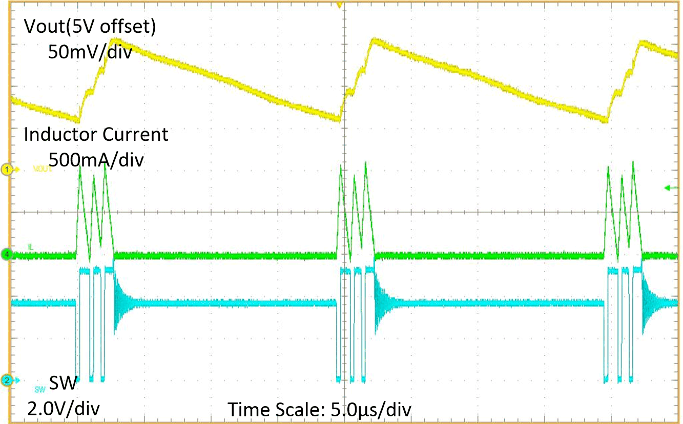
GUID-0877C468-0004-4F76-ACB0-52DCD34EAF0F-low.gif
VIN = 3.6 V, VOUT = 5 V, IOUT = 50 mA
Figure 8-4 Switching Waveform at Light Load
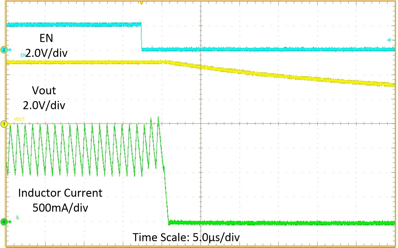
GUID-05BF208D-917E-4FA5-BA0D-A614D31822E9-low.gif
VIN = 3.6 V, VOUT = 5 V, 5-Ω resistance load
Figure 8-6 Shutdown Waveform
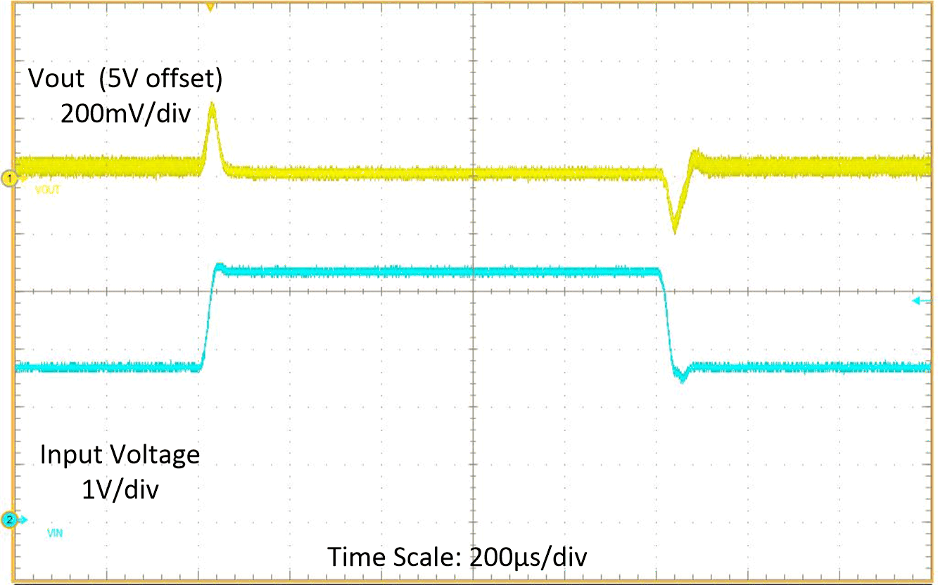
GUID-AD9E80A3-CA1A-44A7-88AA-2C9754DF1444-low.gif
VIN = 2.7 V to 4.35 V with 20-μs slew rate, VOUT = 5 V
IOUT = 1 A
Figure 8-8 Line Transient
GUID-5E10218E-80DE-4A17-82F7-362A6CC83E21-low.gif
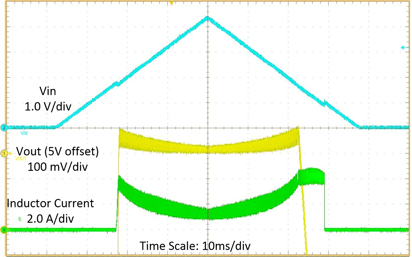
VIN = 0 V to 4.35 V Sweep, VOUT = 5 V, 5-Ω resistance load
Figure 8-10 Line Sweep
GUID-B15F04BB-837C-4885-96E4-A1D1E1EDC420-low.gif
VIN = 3.6 V, VOUT = 5 V, IOUT = 1 A
Figure 8-12 Output Short Protection (Recover)