SGLS276D January 2005 – March 2016 TPS61040-Q1 , TPS61041-Q1
PRODUCTION DATA.
- 1 Features
- 2 Applications
- 3 Description
- 4 Revision History
- 5 Pin Configuration and Functions
- 6 Specifications
- 7 Detailed Description
- 8 Application and Implementation
- 9 Power Supply Recommendations
- 10Layout
- 11Device and Documentation Support
- 12Mechanical, Packaging, and Orderable Information
8 Application and Implementation
NOTE
Information in the following applications sections is not part of the TI component specification, and TI does not warrant its accuracy or completeness. TI’s customers are responsible for determining suitability of components for their purposes. Customers should validate and test their design implementation to confirm system functionality.
8.1 Application Information
The TPS6104x-Q1 is designed for output voltages up to 28 V with an input voltage range of 1.8 V to 6 V. TPS61040-Q1 can operate up to 400-mA typical peak load current and TPS61040-Q1 can operate up to 250-mA typical peak load current. The device operates in a pulse-frequency-modulation (PFM) scheme with constant peak-current control. This control scheme maintains high efficiency over the entire load current range, and with a switching frequency up to 1 MHz, the device enables the use of very small external components.
8.2 Typical Application
The following section provides a step-by-step design approach for configuring the TPS61040-Q1 as a voltage-regulating boost converter for LCD bias supply, as shown in Figure 12.
 Figure 12. LCD Bias Supply
8.2.1 Design Requirements
Table 2 lists the design parameters for this example.
Table 2. Design Parameters
| DESIGN PARAMETER | EXAMPLE VALUE |
|---|---|
| Input Voltage | 1.8 V to 6 V |
| Output Voltage | 18 V |
| Output Current | 10 mA |
8.2.2 Detailed Design Procedure
8.2.2.1 Inductor Selection, Maximum Load Current
Because the PFM peak-current control scheme is inherently stable, the inductor value does not affect the stability of the regulator. The selection of the inductor together with the nominal load current, input and output voltage of the application determines the switching frequency of the converter. Depending on the application, TI recommends inductor values from 2.2 µH to 47 µH. The maximum inductor value is determined by the maximum ON-time of the switch, typically 6 µs. The peak current limit of 400 mA (typically) must be reached within this
6-µs period for proper operation.
The inductor value determines the maximum switching frequency of the converter. Therefore, select the inductor value that ensures the maximum switching frequency at the converter maximum load current is not exceeded. The maximum switching frequency is calculated using Equation 2.

where
- IP = Peak current as described in Peak Current Control
- L = Selected inductor value
- VIN(min) = The highest switching frequency occurs at the minimum input voltage
If the selected inductor value does not exceed the maximum switching frequency of the converter, the next step is to calculate the switching frequency at the nominal load current using Equation 3:

where
- IP = Peak current as described in Peak Current Control
- L = Selected inductor value
- Iload = Nominal load current
- Vd = Rectifier diode forward voltage (typically 0.3 V)
A smaller inductor value gives a higher converter switching frequency, but lowers the efficiency.
The inductor value has less effect on the maximum available load current and is only of secondary order. The best way to calculate the maximum available load current under certain operating conditions is to estimate the expected converter efficiency at the maximum load current. This number can be taken out of the efficiency graphs shown in Figure 1, Figure 2, Figure 3, and Figure 4. The maximum load current can then be estimated using Equation 4.

where
- IP = Peak current as described in Peak Current Control
- L = Selected inductor value
- fS(max) = Maximum switching frequency as calculated previously
- η = Expected converter efficiency. Typically 70% to 85%.
The maximum load current of the converter is the current at the operation point where the converter starts to enter the continuous conduction mode. Usually the converter should always operate in discontinuous conduction mode.
Last, the selected inductor must have a saturation current that exceeds the maximum peak current of the converter (as calculated in Peak Current Control). Use the maximum value for ILIM for this calculation.
Another important inductor parameter is the DC resistance. The lower the DC resistance, the higher the efficiency of the converter. Table 3 lists few typical inductors for LCD Bias Supply design (see Figure 12), but customers must verify and validate them to check whether they are suitable for their application.
Table 3. Typical Inductors for LCD Bias Supply (see Figure 12)
8.2.2.2 Setting The Output Voltage and Feed-Forward Capacitor
The output voltage is calculated as:

For battery-powered applications, a high impedance voltage divider must be used with a typical value for R2 of ≤200 kΩ and a maximum value for R1 of 2.2 MΩ. Smaller values can be used to reduce the noise sensitivity of the feedback pin.
A feed-forward capacitor across the upper feedback resistor R1 is required to provide sufficient overdrive for the error comparator. Without a feed-forward capacitor, or one whose value is too small, the TPS6104x-Q1 shows double pulses or a pulse burst instead of single pulses at the switch node (SW), causing higher output voltage ripple. If this higher output voltage ripple is acceptable, the feed-forward capacitor can be left out.
The lower the switching frequency of the converter, the larger the feed-forward capacitor value required. A good starting point is to use a 10-pF feed-forward capacitor. As a first estimation, the required value for the feed-forward capacitor at the operation point can also be calculated using Equation 6.

where
- R1 = Upper resistor of voltage divider
- fS = Switching frequency of the converter at the nominal load current (see Inductor Selection, Maximum Load Current for calculating the switching frequency)
- CFF = Choose a value that comes closest to the result of the calculation
The larger the feed-forward capacitor the worse the line regulation of the device. Therefore, when concern for line regulation is paramount, the selected feed-forward capacitor must be as small as possible. See the next section for more information about line and load regulation.
8.2.2.3 Line and Load Regulation
The line regulation of the TPS6104x-Q1 depends on the voltage ripple on the feedback pin. Usually a 50-mV peak-to-peak voltage ripple on the feedback pin FB gives good results.
Some applications require a very tight line regulation and can only allow a small change in output voltage over a certain input voltage range. If no feed-forward capacitor CFF is used across the upper resistor of the voltage feedback divider, the device has the best line regulation. Without the feed-forward capacitor the output voltage ripple is higher because the TPS6104x-Q1 shows output voltage bursts instead of single pulses on the switch pin (SW), increasing the output voltage ripple. Increasing the output capacitor value reduces the output voltage ripple.
If a larger output capacitor value is not an option, a feed-forward capacitor CFF can be used as described in the previous section. The use of a feed-forward capacitor increases the amount of voltage ripple present on the feedback pin (FB). The greater the voltage ripple on the feedback pin (≥50 mV), the worse the line regulation. There are two ways to improve the line regulation further:
- Use a smaller inductor value to increase the switching frequency which will lower the output voltage ripple, as well as the voltage ripple on the feedback pin.
- Add a small capacitor from the feedback pin (FB) to ground to reduce the voltage ripple on the feedback pin down to 50 mV again. As a starting point, the same capacitor value as selected for the feed-forward capacitor CFF can be used.
8.2.2.4 Output Capacitor Selection
For best output voltage filtering, TI recommends a low ESR output capacitor. Ceramic capacitors have a low ESR value but tantalum capacitors can be used as well, depending on the application.
Assuming the converter does not show double pulses or pulse bursts on the switch node (SW), the output voltage ripple can be calculated using Equation 7.

where
- IP = Peak current as described in the Peak Current Control section
- L = Selected inductor value
- Iout = Nominal load current
- fS (Iout) = Switching frequency at the nominal load current as calculated previously
- Vd = Rectifier diode forward voltage (typically 0.3 V)
- Cout = Selected output capacitor
- ESR = Output capacitor ESR value
Table 4 lists few typical capacitors for LCD Bias Supply design (see Figure 12), but customers must verify and validate them to check whether they are suitable for their application.
Table 4. Typical Input and Output Capacitors for LCD Bias Supply Design (See Figure 12)
| DEVICE | CAPACITOR | VOLTAGE RATING | COMPONENT SUPPLIER | COMMENTS |
|---|---|---|---|---|
| TPS6104x-Q1 | 4.7 μF/X5R/0805 | 6.3 V | Taiyo Yuden JMK212BY475MG | CIN |
| 10 μF/X5R/0805 | 6.3 V | Taiyo Yuden JMK212BJ106MG | CIN | |
| 1 μF/X7R/1206 | 25 V | Taiyo Yuden TMK316BJ105KL | COUT | |
| 1 μF/X5R/1206 | 35 V | Taiyo Yuden GMK316BJ105KL | COUT | |
| 4.7 μF/X5R/1210 | 25 V | Taiyo Yuden TMK325BJ475MG | COUT |
8.2.2.5 Input Capacitor Selection
For good input voltage filtering, TI recommends low-ESR ceramic capacitors. A 4.7-μF ceramic input capacitor is sufficient for most of the applications. For better input voltage filtering this value can be increased. See Table 4 and the Typical Application section for input capacitor recommendations.
8.2.2.6 Diode Selection
To achieve high efficiency, a Schottky diode must be used. The current rating of the diode must meet the peak current rating of the converter as it is calculated in the section peak current control. Use the maximum value for ILIM for this calculation. Table 5 lists the few typical Schottky Diodes for LCD Bias Supply design shown in Figure 12. Customers must verify and validate them, however, to check whether they are suitable for their application.
Table 5. Typical Schottky Diodes for LCD Bias Supply Design (See Figure 12)
| DEVICE | REVERSE VOLTAGE | COMPONENT SUPPLIER | COMMENTS |
|---|---|---|---|
| TPS6104x-Q1 | 30 V | ON Semiconductor MBR0530 | |
| 20 V | ON Semiconductor MBR0520 | ||
| 20 V | ON Semiconductor MBRM120L | High efficiency | |
| 30 V | Toshiba CRS02 |
8.2.3 Application Curves
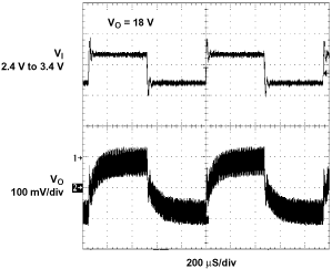
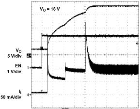
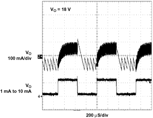
8.3 System Examples
Figure 16 to Figure 22 shows the different possible power supply designs with the TPS6104x-Q1 devices. However, these circuits must be fully validated and tested by customers before they actually use them in their designs. TI does not warrant the accuracy or completeness of these circuits, nor does TI accept any responsibility for them.
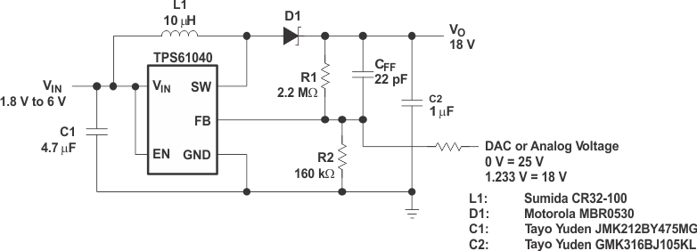 Figure 16. LCD Bias Supply With Adjustable Output Voltage
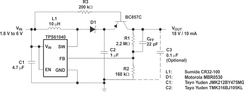 Figure 17. LCD Bias Supply With Load Disconnect
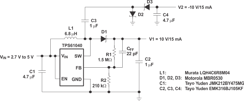 Figure 18. Positive and Negative Output LCD Bias Supply
 Figure 19. Standard 3.3-V to 12-V Supply
 Figure 20. Dual Battery Cell to 5-V/50-mA Conversion
 Efficiency Approximately Equals 84% at VIN = 2.4 V to VO = 5 V/45 mA
 Figure 21. White-LED Supply With Adjustable Brightness Control
 Using a PWM Signal on the Enable Pin Efficiency Approx. Equals 86% at VIN = 3 V, ILED = 15 mA
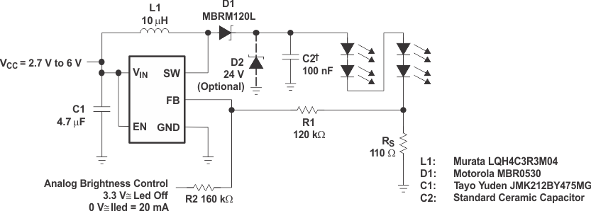
Using an Analog Signal on the Feedback Pin