SGLS276D January 2005 – March 2016 TPS61040-Q1 , TPS61041-Q1
PRODUCTION DATA.
- 1 Features
- 2 Applications
- 3 Description
- 4 Revision History
- 5 Pin Configuration and Functions
- 6 Specifications
- 7 Detailed Description
- 8 Application and Implementation
- 9 Power Supply Recommendations
- 10Layout
- 11Device and Documentation Support
- 12Mechanical, Packaging, and Orderable Information
7 Detailed Description
7.1 Overview
The TPS6104x-Q1 is a high-frequency boost converter dedicated for small-to-medium LCD bias supply and white-LED backlight supplies. The device is ideal for generating output voltages up to 28 V from a dual-cell NiMH/NiCd or a single-cell device Li-Ion battery.
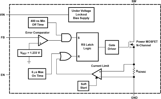
7.2 Functional Block Diagram

7.3 Feature Description
7.3.1 Peak Current Control
The internal switch turns on until the inductor current reaches the typical DC current limit (ILIM) of 400 mA (TPS61040-Q1) or 250 mA (TPS61041-Q1). Due to the internal propagation delay of typical 100 ns, the actual current exceeds the DC-current limit threshold by a small amount. The typical peak current limit can be calculated:

where
- VIN= Input voltage
- L= Selected inductor value
- ILIM = Typical DC current limit
The higher the input voltage and the lower the inductor value, the greater the peak.
By selecting the TPS6104x-Q1, it is possible to tailor the design to the specific application current limit requirements. A lower current limit supports applications requiring lower output power and allows the use of an inductor with a lower current rating and a smaller form factor. A lower current limit usually has a lower output-voltage ripple as well.
7.3.2 Soft Start
All inductive step-up converters exhibit high inrush current during start-up if no special precaution is made. This can cause voltage drops at the input rail during start-up and may result in an unwanted or early system shutdown.
The TPS6104x-Q1 limits this inrush current by increasing the current limit in two steps starting from for 256 cycles to
  for the next 256 cycles, and then full current limit (see Figure 15).
7.3.3 Enable
Pulling the enable (EN) to ground shuts down the device reducing the shutdown current to 1 µA (typical). Because there is a conductive path from the input to the output through the inductor and Schottky diode, the output voltage is equal to the input voltage during shutdown. The enable pin must be terminated and must not be left floating. Using a small external transistor disconnects the input from the output during shutdown as shown in Figure 17.
7.3.4 Undervoltage Lockout
An undervoltage lockout prevents misoperation of the device at input voltages below typical 1.5 V. When the input voltage is below the undervoltage threshold the main switch is turned off.
7.3.5 Thermal Shutdown
An internal thermal shutdown is implemented and turns off the internal MOSFETs when the typical junction temperature of 168°C is exceeded. The thermal shutdown has a hysteresis of typically 25°C. This data is based on statistical means and is not tested during the regular mass production of the IC.
7.4 Device Functional Modes
The TPS6104x-Q1 operates with an input voltage range of 1.8 V to 6 V and can generate output voltages up to 28 V. The device operates in a pulse frequency modulation (PFM) scheme with constant peak current control. This control scheme maintains high efficiency over the entire load current range, and with a switching frequency up to 1 MHz, the device enables the use of very small external components.
The converter monitors the output voltage, and as soon as the feedback voltage falls below the reference voltage of typically 1.233 V, the internal switch turns on and the current ramps up. The switch turns off as soon as the inductor current reaches the internally set peak current of typically 400 mA (TPS61040-Q1) or 250 mA (TPS61041-Q1). See Peak Current Control for more information. The second criteria that turns off the switch is the maximum ON-time of 6 µs (typical). This is just to limit the maximum ON-time of the converter to cover for extreme conditions. As the switch is turned off, the external Schottky diode is forward biased delivering the current to the output. The switch remains off for a minimum of 400 ns (typical), or until the feedback voltage drops below the reference voltage again. Using this PFM peak-current control scheme, the converter operates in discontinuous conduction mode (DCM) where the switching frequency depends on the output current, which results in high efficiency over the entire load current range. This regulation scheme is inherently stable, allowing a wider selection range for the inductor and output capacitor.