ZHCSDL4 April 2015 TPS61046
PRODUCTION DATA.
- 1 特性
- 2 应用
- 3 说明
- 4 简化电路原理图
- 5 修订历史记录
- 6 Pin Configuration and Functions
- 7 Specifications
- 8 Detailed Description
- 9 Application and Implementation
- 10Power Supply Recommendations
- 11Layout
- 12器件和文档支持
- 13机械封装和可订购信息
9 Application and Implementation
9.1 Application Information
The TPS61046 is a boost DC-DC converter with a PWM switch, a power diode and an input/output isolation switch integrated. The device supports up to 28-V output with the input range from 1.8 V to 5.5 V. The TPS61046 adopts the current-mode control with adaptive constant off-time. The switching frequency is quasi-constant at 1.0 MHz. The isolation switch disconnects the output from the input during shutdown to minimize leakage current.
The following design procedure can be used to select component values for the TPS61046.
9.2 Typical Application - 12-V Output Boost Converter
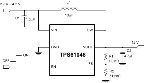 Figure 11. 12-V Boost Converter
9.2.1 Design Requirements
Table 1. Design Requirements
| PARAMETERS | VALUES |
|---|---|
| Input Voltage | 2.7 V ~ 4.2 V |
| Output Voltage | 12 V |
| Output Current | 50 mA |
| Output Voltage Ripple | ±50mV |
9.2.2 Detailed Design Procedure
9.2.2.1 Programming the Output Voltage
There are two ways to set the output voltage of the TPS61046. When the FB pin is connected to the input voltage, the output voltage is fixed to 12 V. This function makes the TPS61046 only need three external components to minimize the solution size. The second way is to use an external resistor divider to set the desired output voltage.
By selecting the external resistor divider R1 and R2, as shown in Equation 1, the output voltage is programmed to the desired value. When the output voltage is regulated, the typical voltage at the FB pin is VREF of 795 mV.

Where:
VOUT is the desired output voltage
VREF is the internal reference voltage at the FB pin
For best accuracy, R2 should be kept smaller than 80 kΩ to ensure the current flowing through R2 is at least 100 times larger than the FB pin leakage current. Changing R2 towards a lower value increases the immunity against noise injection. Changing the R2 towards a higher value reduces the quiescent current for achieving highest efficiency at low load currents.
9.2.2.2 Inductor Selection
Because the selection of the inductor affects steady state operation, transient behavior, and loop stability, the inductor is the most important component in power regulator design. There are three important inductor specifications, inductor value, saturation current, and dc resistance (DCR).
The TPS61046 is designed to work with inductor values between 1.0 µH and 22 µH. Follow Equation 2 to Equation 4 to calculate the inductor’s peak current for the application. To calculate the current in the worst case, use the minimum input voltage, maximum output voltage, and maximum load current of the application. To have enough design margin, choose the inductor value with -30% tolerance, and a low power-conversion efficiency for the calculation.
In a boost regulator, the inductor dc current can be calculated with Equation 2.

Where:
VOUT = output voltage
IOUT = output current
VIN = input voltage
η = power conversion efficiency, use 80% for most applications
The inductor ripple current is calculated with the Equation 3 for an asynchronous boost converter in continuous conduction mode (CCM).

Where:
ΔIL(P-P) = inductor ripple current
L = inductor value
fSW = switching frequency
VOUT = output voltage
VIN = input voltage
Therefore, the inductor peak current is calculated with Equation 4.

Normally, it is advisable to work with an inductor peak-to-peak current of less than 40% of the average inductor current for maximum output current. A smaller ripple from a larger valued inductor reduces the magnetic hysteresis losses in the inductor and EMI. Bit in the same way, load transient response time is increased. Because the TPS61046 is for relatively small output current application, the inductor peak-to-peak current could be as high as 200% of the average current with a small inductor value, which means the TPS61046 always works in DCM mode.Table 2 lists the recommended inductor for the TPS61046.
Table 2. Recommended Inductors for the TPS61046
| PART NUMBER | L(µH) | DCR MAX (mΩ) | SATURATION CURRENT (A) | SIZE (LxWxH) | VENDOR |
|---|---|---|---|---|---|
| FDSD0420-H-100M | 10 | 200 | 2.5 | 4.2x4.2x2.0 | Toko |
| CDRH3D23/HP | 10 | 198 | 1.02 | 4.0x4.0x2.5 | Sumida |
| 1239AS-H-100M | 10 | 460 | 1.0 | 2.5x2.0x1.2 | Toko |
| VLS4012-4R7M | 4.7 | 132 | 1.1 | 4.0x4.0x1.2 | TDK |
| 0420CDMCBDS | 22 | 379 | 1.6 | 4.5x4.1x2.0 | Sumida |
9.2.2.3 Input and Output Capacitor Selection
The output capacitor is mainly selected to meet the requirements for output ripple and loop stability. This ripple voltage is related to the capacitor’s capacitance and its equivalent series resistance (ESR). Assuming a ceramic capacitor with zero ESR, the minimum capacitance needed for a given ripple can be calculated by:

Where:
DMAX = maximum switching duty cycle
VRIPPLE = peak to peak output voltage ripple
The ESR impact on the output ripple must be considered if tantalum or aluminum electrolytic capacitors are used.
Care must be taken when evaluating a ceramic capacitor’s derating under dc bias, aging, and ac signal. For example, the dc bias can significantly reduce capacitance. A ceramic capacitor can lose more than 50% of its capacitance at its rated voltage. Therefore, always leave margin on the voltage rating to ensure adequate capacitance at the required output voltage.
It is recommended to use the output capacitor with effective capacitance in the range of 0.47 μF to 10 μF. The output capacitor affects the small signal control loop stability of the boost regulator. If the output capacitor is below the range, the boost regulator can potentially become unstable. Increasing the output capacitor makes the output voltage ripple smaller in PWM mode.
For input capacitor, a ceramic capacitor with more than 1.0 µF is enough for most applications.
9.2.3 Application Performance Curves
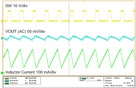
| VIN = 3.6 V, VOUT = 12 V, IOUT = 50 mA | ||
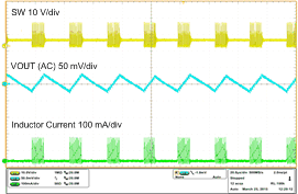
| VIN = 3.6 V, VOUT = 12 V, IOUT = 3 mA | ||
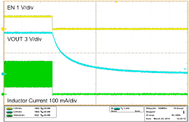
| VIN = 3.6 V, VOUT = 12 V, IOUT = 50 mA | ||
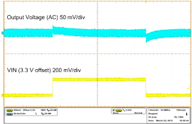
| VOUT = 12V, IOUT = 50 mA | ||
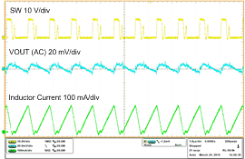
| VIN = 3.6 V, VOUT = 12 V, IOUT = 20 mA | ||
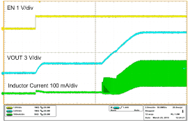
| VIN = 3.6 V, VOUT = 12 V, IOUT = 50 mA | ||
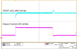
| VIN = 3.6 V, VOUT = 12 V | ||
9.3 System Examples
9.3.1 Fixed 12-V Output Voltage with Three External Components
The TPS61046 can output fixed 12-V voltage by connecting the FB pin to the VIN pin to save the external resistor divider. The Figure 19 shows the application circuit.
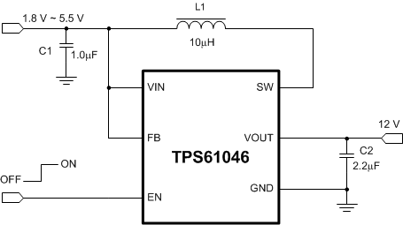 Figure 19. Fixed 12-V Output Voltage by Connecting the FB Pin to VIN Pin