SLVSAA5A May 2010 – December 2015 TPS61071-Q1
UNLESS OTHERWISE NOTED, this document contains PRODUCTION DATA.
- 1 Features
- 2 Applications
- 3 Description
- 4 Revision History
- 5 Pin Configuration and Functions
- 6 Specifications
- 7 Detailed Description
- 8 Application and Implementation
- 9 Power Supply Recommendations
- 10Layout
- 11Device and Documentation Support
- 12Mechanical, Packaging, and Orderable Information
7 Detailed Description
7.1 Overview
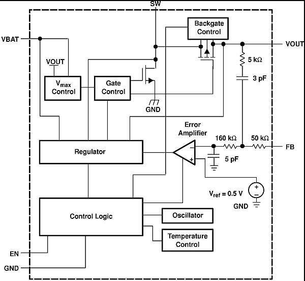
The TPS61071-Q1 provides a boost power supply solution for products powered by either DC supply rails or batteries such as one-cell, two-cell, or three-cell alkaline, NiCd or NiMH, or one-cell Li-ion or Li-polymer battery. Output currents can go as high as 75 mA, while using a single-cell alkaline, and discharge down to 0.9 V. The device can also generate 5 V at 200 mA from a 3.3-V rail or a Li-ion battery. The boost converter is based on a fixed frequency, pulse-width modulation (PWM) controller using a synchronous rectifier to obtain maximum efficiency. The TPS61071-Q1 does not have a POWER-SAVE mode. Even with low-load currents, the device is forced to operate at the fixed switching frequency. The maximum peak current in the boost switch is limited typically to a value of 600 mA. An external-resistor divider programs the output voltage. To minimize battery drain, disable the converter. During shutdown, the load disconnects from the battery.
7.2 Functional Block Diagram

7.3 Feature Description
7.3.1 Controller Circuit
The controller circuit of the device is based on a fixed-frequency multiple feed-forward controller topology. Input voltage, output voltage, and voltage drop on the NMOS switch are monitored and forwarded to the regulator. So, changes in the operating conditions of the converter directly affect the duty cycle and must not take the indirect and slow way through the control loop and the error amplifier. The control loop, determined by the error amplifier, only has to handle small signal errors. The input for it is the feedback voltage on the FB pin. It is compared with the internal reference voltage to generate an accurate and stable output voltage.
The peak current of the NMOS switch is also sensed to limit the maximum current flowing through the switch and the inductor. The typical peak-current limit is set to 600 mA. An internal temperature sensor prevents the device from getting overheated in case of excessive power dissipation.
7.3.1.1 Synchronous Rectifier
The device integrates an N-channel and a P-channel MOSFET transistor to realize a synchronous rectifier. Because the commonly used discrete Schottky rectifier is replaced with a low RDS(on) PMOS switch, the power conversion efficiency reaches values above 90%. A special circuit is applied to disconnect the load from the input during shutdown of the converter. In conventional synchronous rectifier circuits, the backgate diode of the high-side PMOS is forward biased in shutdown and allows current flowing from the battery to the output. However, this device uses a special circuit, which takes the cathode of the backgate diode of the high-side PMOS and disconnects it from the source when the regulator is not enabled (EN = low).
The benefit of this feature for the system design engineer is that the battery is not depleted during shutdown of the converter. No additional components must be added to the design to make sure that the battery is disconnected from the output of the converter.
7.3.1.2 Undervoltage Lockout
An undervoltage lockout function prevents the device from operating if the supply voltage on VBAT is lower than approximately 0.8 V. When in operation and the battery is being discharged, the device automatically enters the shutdown mode if the voltage on VBAT drops below approximately 0.8 V. This undervoltage lockout function is implemented in order to prevent the malfunctioning of the converter.
7.3.1.3 Soft Start and Short-Circuit Protection
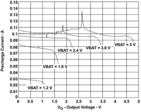
When the device enables, the internal start-up cycle starts with the first step, the precharge phase. During precharge, the rectifying switch is turned on until the output capacitor is charged to a value close to the input voltage. The rectifying switch is current limited during this phase. The current limit increases with the output voltage. This circuit also limits the output current under short-circuit conditions at the output. Figure 18 shows the typical precharge current vs output voltage for specific input voltages:
 Figure 18. Precharge and Short Circuit Current
After charging the output capacitor to the input voltage, the device starts switching. If the input voltage is below 1.8 V, the device works with a fixed duty cycle of 70% until the output voltage reaches 1.8 V. After that the duty cycle is set depending on the input output voltage ratio. Until the output voltage reaches its nominal value, the boost switch current limit is set to 50% of its nominal value to avoid high peak currents at the battery during start-up. As soon as the output voltage is reached, the regulator takes control, and the switch current limit is set back to 100%.
7.4 Device Functional Modes
7.4.1 Device Enable
The device is put into operation when EN is set high and put into a SHUTDOWN mode when EN is set to GND. In SHUTDOWN mode, the regulator stops switching, all internal control circuitry switches off, and the device isolates the load from the input (see Synchronous Rectifier). This also means that the output voltage can drop below the input voltage during shutdown. During start-up of the converter, the duty cycle and the peak current are limited to avoid high-peak currents drawn from the battery.