SLVSAA5A May 2010 – December 2015 TPS61071-Q1
UNLESS OTHERWISE NOTED, this document contains PRODUCTION DATA.
- 1 Features
- 2 Applications
- 3 Description
- 4 Revision History
- 5 Pin Configuration and Functions
- 6 Specifications
- 7 Detailed Description
- 8 Application and Implementation
- 9 Power Supply Recommendations
- 10Layout
- 11Device and Documentation Support
- 12Mechanical, Packaging, and Orderable Information
6 Specifications
6.1 Absolute Maximum Ratings
over operating free-air temperature range (unless otherwise noted)(1)| MIN | MAX | UNIT | |
|---|---|---|---|
| Input voltage range on SW, VOUT, VBAT, EN, FB | –0.3 | 7 | V |
| Operating virtual junction temperature, TJ | –40 | 150 | °C |
| Storage temperature, Tstg | –65 | 150 | °C |
(1) Stresses beyond those listed under Absolute Maximum Ratings may cause permanent damage to the device. These are stress ratings only, and functional operation of the device at these or any other conditions beyond those indicated under Recommended Operating Conditions is not implied. Exposure to absolute-maximum-rated conditions for extended periods may affect device reliability.
6.2 ESD Ratings
| VALUE | UNIT | |||
|---|---|---|---|---|
| V(ESD) | Electrostatic discharge | Human-body model (HBM), per AEC Q100-002(1) | ±2000 | V |
| Charged-device model (CDM), per AEC Q100-011 | ±1000 | |||
(1) AEC Q100-002 indicates that HBM stressing shall be in accordance with the ANSI/ESDA/JEDEC JS-001 specification.
6.3 Recommended Operating Conditions
| MIN | NOM | MAX | UNIT | |
|---|---|---|---|---|
| Supply voltage at VBAT, VI | 0.9 | 5.5 | V | |
| Operating free air temperature range, TA | –40 | 105 | °C | |
| Operating virtual junction temperature range, TJ | –40 | 125 | °C |
6.4 Thermal Information
| THERMAL METRIC(1) | TPS61071-Q1 | UNIT | |
|---|---|---|---|
| DDC (SOT) | |||
| 6 PINS | |||
| RθJA | Junction-to-ambient thermal resistance | 139.1 | °C/W |
| RθJC(top) | Junction-to-case (top) thermal resistance | 34.8 | °C/W |
| RθJB | Junction-to-board thermal resistance | 42.5 | °C/W |
| ψJT | Junction-to-top characterization parameter | 1.4 | °C/W |
| ψJB | Junction-to-board characterization parameter | 40.7 | °C/W |
| RθJC(bot) | Junction-to-case (bottom) thermal resistance | N/A | °C/W |
(1) For more information about traditional and new thermal metrics, see the Semiconductor and IC Package Thermal Metrics application report, SPRA953.
6.5 Electrical Characteristics
over recommended free-air temperature range and over recommended input voltage range (typical at an ambient temperature range of 25°C) (unless otherwise noted)| PARAMETER | TEST CONDITIONS | MIN | TYP | MAX | UNIT | ||
|---|---|---|---|---|---|---|---|
| DC-DC STAGE | |||||||
| VI | Minimum input voltage range for start-up | RL = 270 Ω | 1.1 | 1.25 | V | ||
| Input voltage range, after start-up | TA = 25°C | 0.9 | 5.5 | ||||
| VO | Output voltage range | 1.8 | 5.5 | V | |||
| V(FB) | Feedback voltage | TA = 25°C | 490 | 500 | 510 | mV | |
| f | Oscillator frequency | 960 | 1200 | 1440 | kHz | ||
| I(SW) | Switch current limit | VOUT= 3.3 V | 455 | 600 | 735 | mA | |
| Start-up current limit | 0.5 × ISW | mA | |||||
| Boost switch-on resistance | VOUT= 3.3 V | 480 | mΩ | ||||
| Rectifying switch-on resistance | VOUT= 3.3 V | 600 | mΩ | ||||
| Total accuracy (including line and load regulation) | 5% | ||||||
| Line regulation | 1% | ||||||
| Load regulation | 1% | ||||||
| Quiescent current | VBAT | IO= 0 mA, V(EN)= VBAT = 1.2 V, VOUT = 3.3 V, TA = 25°C |
0.5 | 1 | µA | ||
| VOUT | 190(1) | 300(1) | |||||
| 20(2) | |||||||
| Shutdown current | V(EN) = 0 V, VBAT = 1.2 V, TA = 25°C | 0.05 | 0.5 | µA | |||
| CONTROL STAGE | |||||||
| V(UVLO) | Undervoltage lockout threshold | V(BAT) voltage decreasing | 0.8 | V | |||
| VIL | EN input low voltage | 0.2 × VBAT | V | ||||
| VIH | EN input high voltage | 0.8 × VBAT | V | ||||
| EN input current | Clamped on GND or VBAT | 0.01 | 0.1 | µA | |||
| Overtemperature protection | 140 | °C | |||||
| Overtemperature hysteresis | 20 | °C | |||||
(1) Switching current
(2) Non-switching current
6.6 Typical Characteristics
Table 1. Table of Graphs
| FIGURE | ||
|---|---|---|
| Maximum output current | vs Input voltage | Figure 1 |
| Efficiency | vs Output current | Figure 2 |
| vs Output current | Figure 3 | |
| vs Output current | Figure 4 | |
| vs Input voltage | Figure 5 | |
| vs Input voltage | Figure 6 | |
| Output voltage | vs Output current | Figure 7 |
| vs Output current | Figure 8 | |
| No load supply current into VOUT | vs Input voltage | Figure 9 |
| Waveforms | Output voltage in continuous mode | Figure 10 |
| Output voltage in continuous mode | Figure 11 | |
| Load transient response | Figure 12 | |
| Load transient response | Figure 13 | |
| Line transient response | Figure 14 | |
| Line transient response | Figure 15 | |
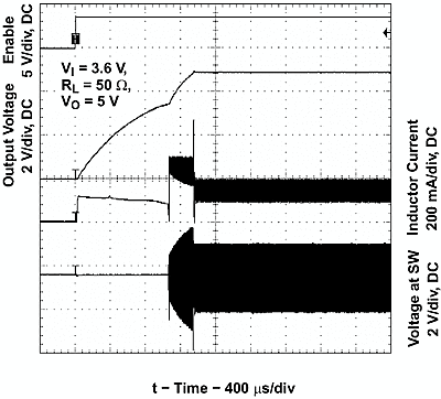
| Start-up after enable | Figure 16 | |
| Start-up after enable | Figure 17 |
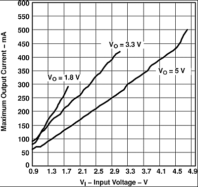 Figure 1. Maximum Output Current vs Input Voltage
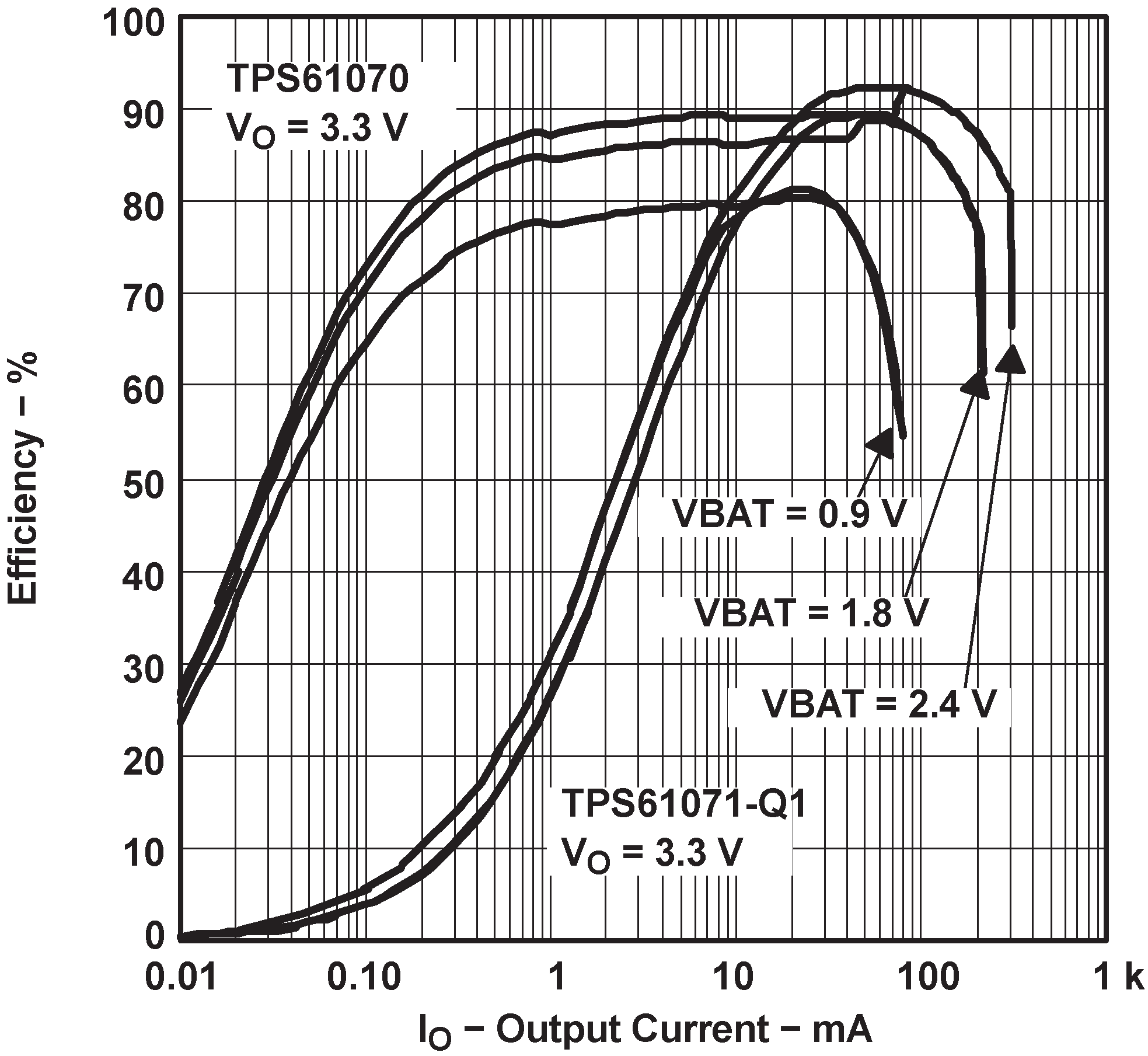 Figure 3. Efficiency vs Output Current
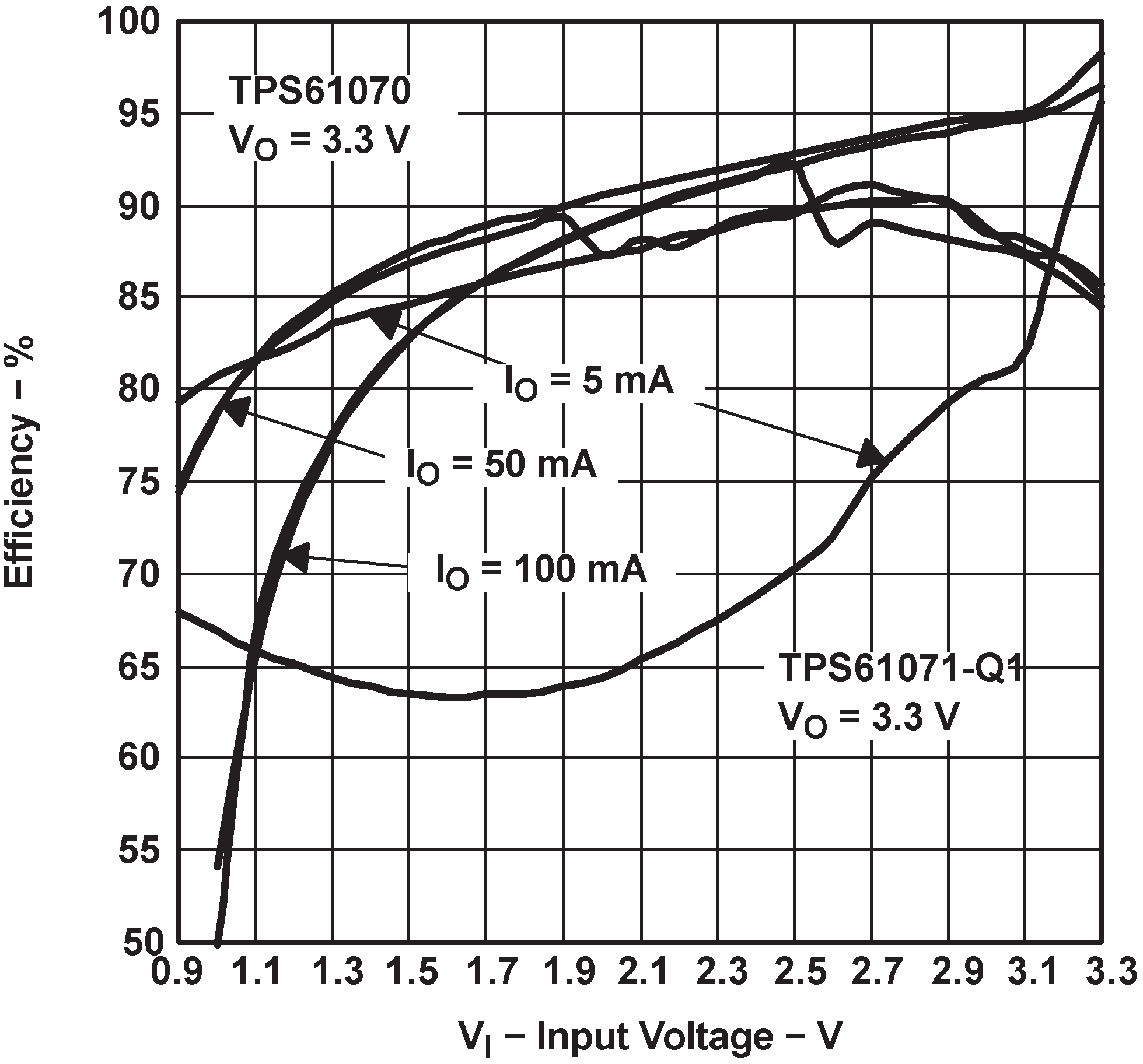 Figure 5. Efficiency vs Input Voltage
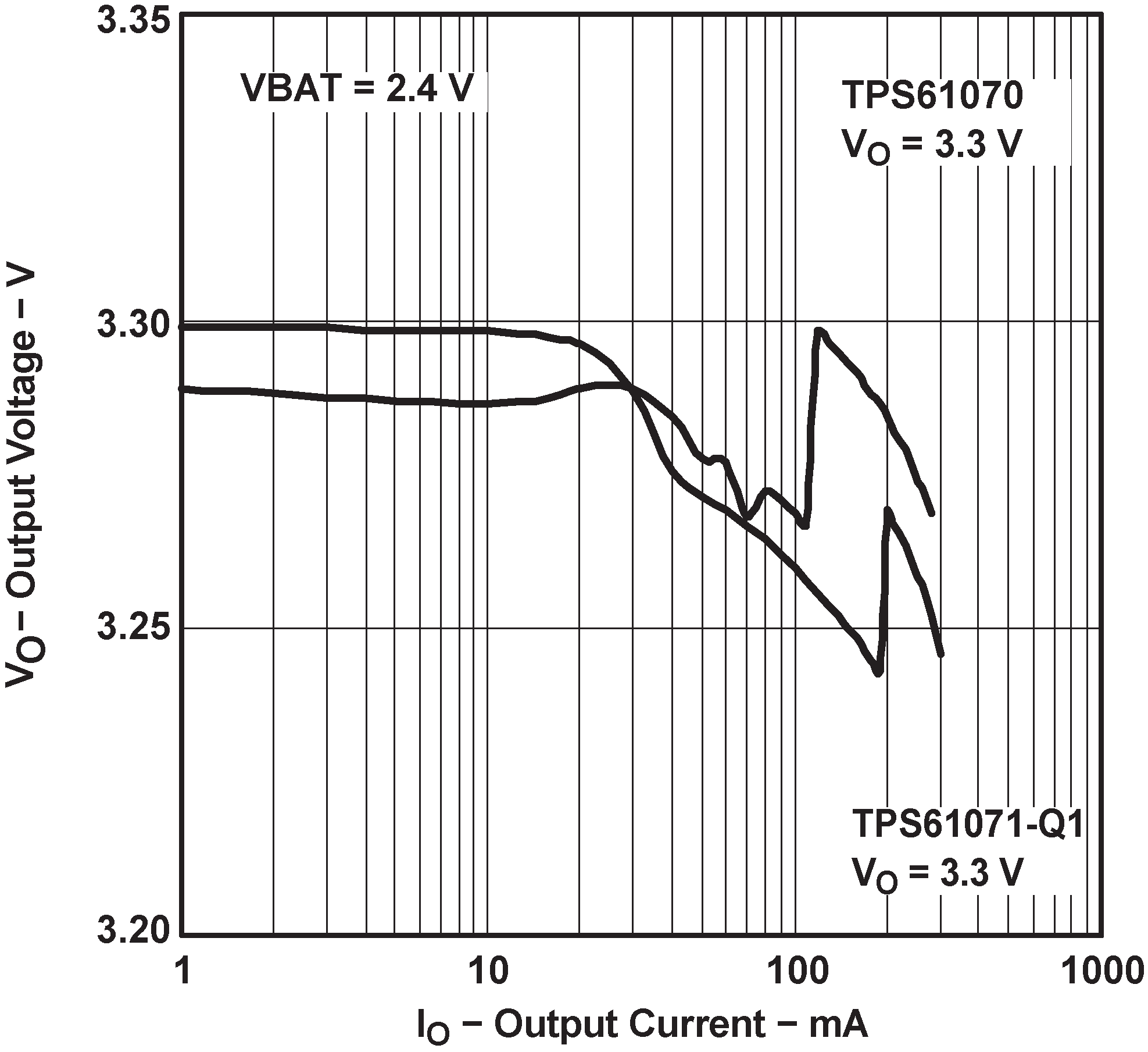 Figure 7. Output Voltage vs Output Current
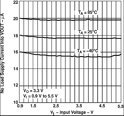 Figure 9. No Load Supply Current Into VOUT vs Input Voltage
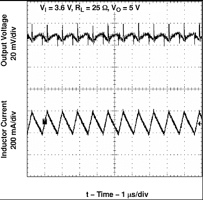 Figure 11. TPS61071 Output Voltage in Continuous Mode
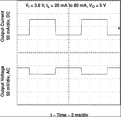 Figure 13. TPS61071 Load Transient Response
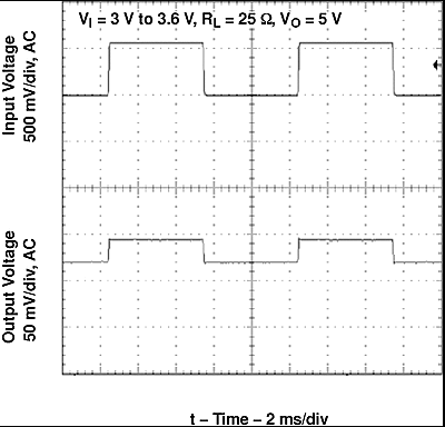 Figure 15. TPS61071 Line Transient Response
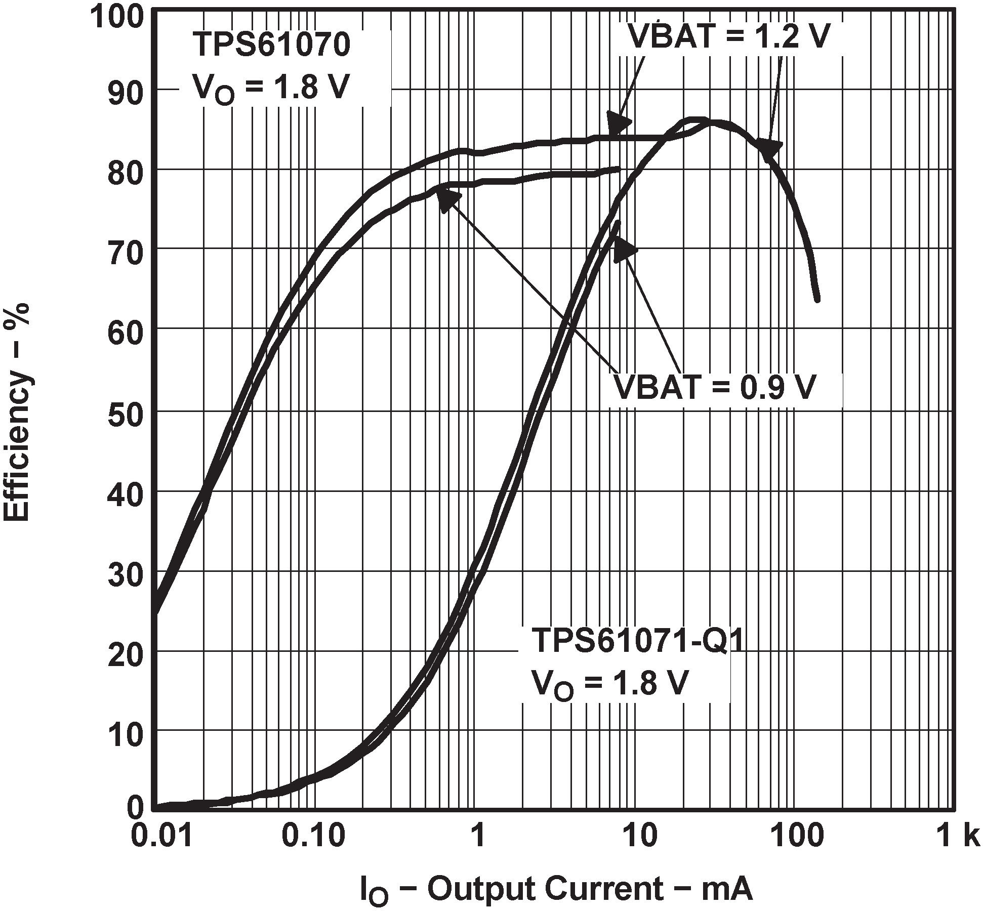 Figure 2. Efficiency vs Output Current
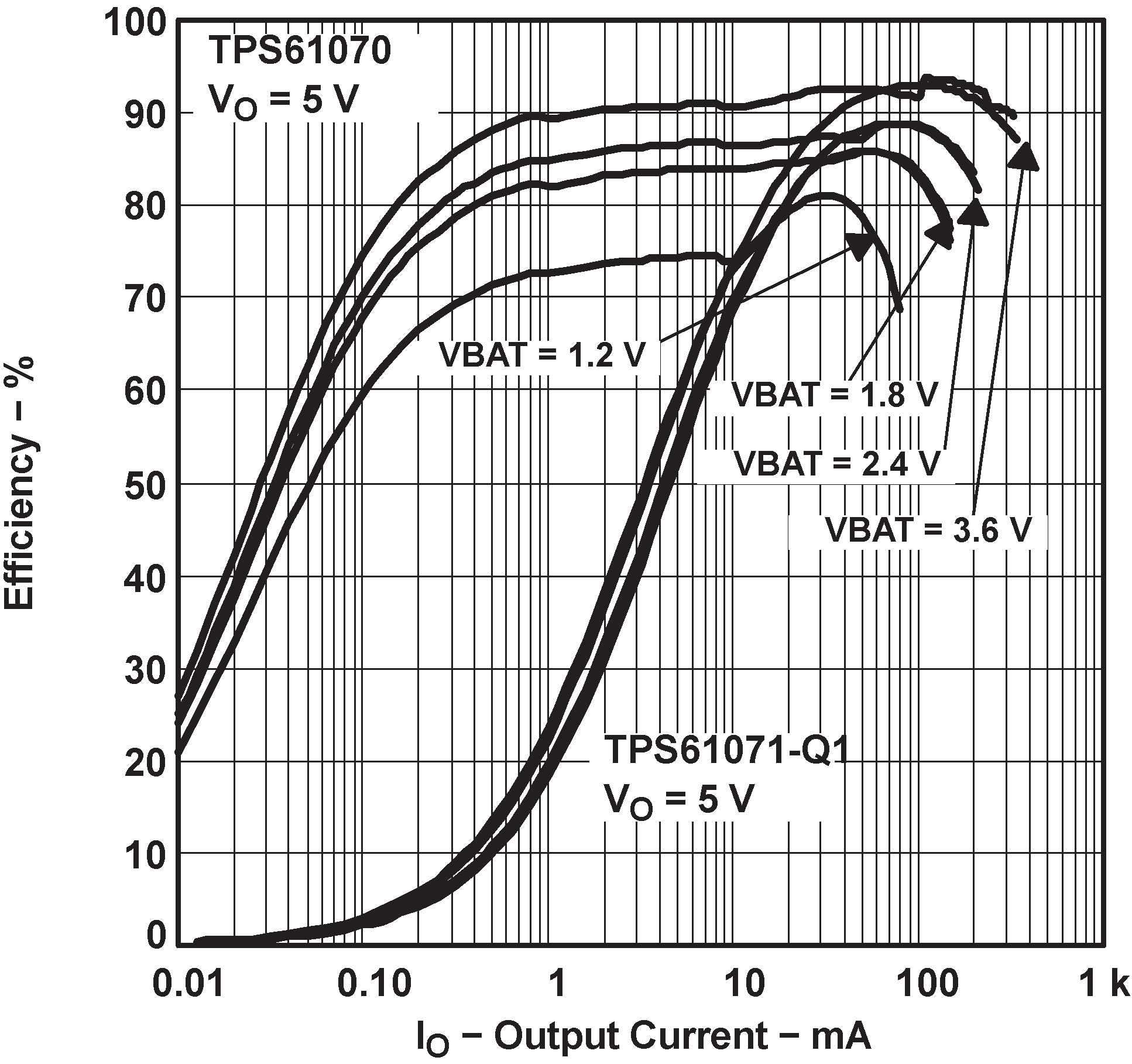 Figure 4. Efficiency vs Output Current
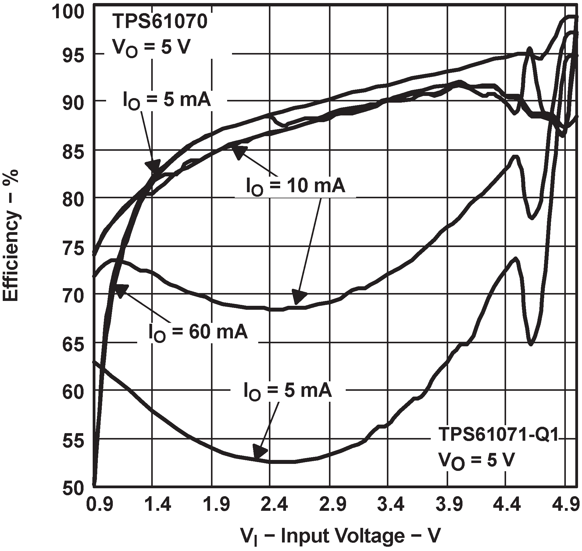 Figure 6. Efficiency vs Input Voltage
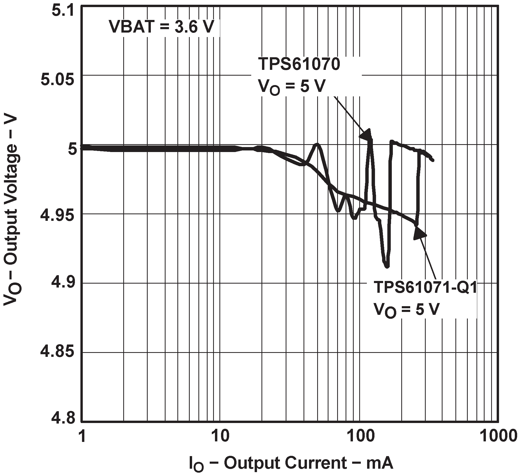 Figure 8. Output Voltage vs Output Current
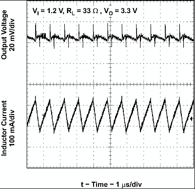 Figure 10. TPS61071 Output Voltage in Continuous Mode
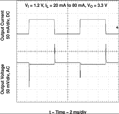 Figure 12. TPS61071 Load Transient Response
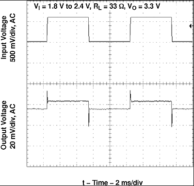 Figure 14. TPS61071 Line Transient Response
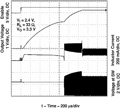 Figure 16. TPS61071 Start-Up After Enable
