SLVSB50C December 2011 – June 2020 TPS61087-Q1
PRODUCTION DATA.
- 1 Features
- 2 Applications
- 3 Description
- 4 Revision History
- 5 Pin Configuration and Functions
- 6 Specifications
- 7 Detailed Description
- 8 Application and Implementation
- 9 Power Supply Recommendations
- 10Layout
- 11Device and Documentation Support
- 12Mechanical, Packaging, and Orderable Information
6.6 Typical Characteristics
The typical characteristics are measured with the inductors 7447789003 3.3 µH (high frequency) or 74454068 6.8 µH (low frequency) from Wurth and the rectifier diode SL22.Table 1. Table of Graphs
| FIGURE | |||
|---|---|---|---|
| IOUT(max) | Maximum load current | vs Input voltage at High frequency (1.2 MHz) | Figure 1 |
| IOUT(max) | Maximum load current | vs Input voltage at Low frequency (650 kHz) | Figure 2 |
| η | Efficiency | vs Load current, VS = 15 V, VIN = 5 V | Figure 3 |
| vs Load current, VS = 9 V, VIN = 3.3 V | Figure 4 | ||
| Supply current | vs Supply voltage | Figure 5 | |
| Oscillator frequency | vs Load current | Figure 6 | |
| Oscillator frequency | vs Supply voltage | Figure 7 | |
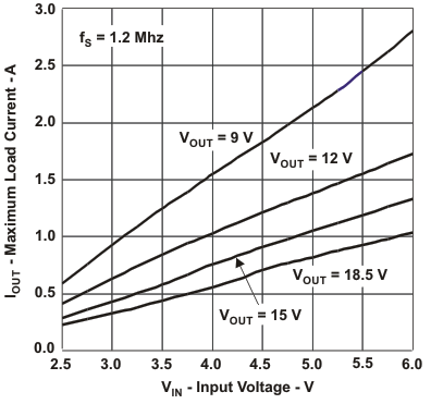 Figure 1. Maximum Load Current vs Input Voltage
 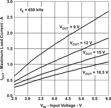 Figure 2. Maximum Load Current vs Input Voltage
 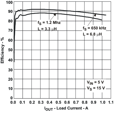 Figure 3. Efficiency vs Load Current
 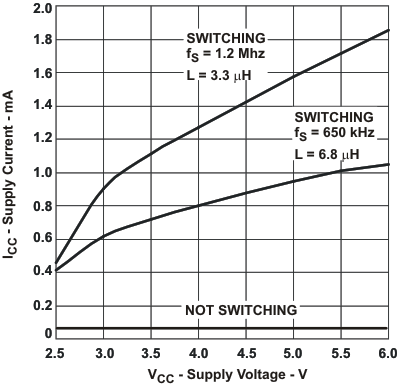 Figure 5. Supply Current vs Supply Voltage
 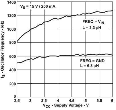 Figure 7. Oscillator Frequency vs Supply Voltage
 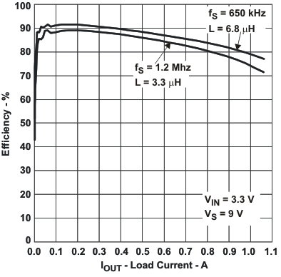 Figure 4. Efficiency vs Load Current
 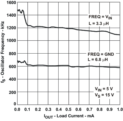 Figure 6. Oscillator Frequency vs Load Current