ZHCSJM5D September   2009  – April 2019 TPS61093

PRODUCTION DATA.  

  1. 特性
  2. 应用
  3. 说明
    1.     Device Images
      1.      简化原理图
  4. 修订历史记录
  5. Pin Configuration and Functions
    1.     Pin Functions
  6. Specifications
    1. 6.1 Absolute Maximum Ratings
    2. 6.2 ESD Ratings
    3. 6.3 Recommended Operating Conditions
    4. 6.4 Thermal Information
    5. 6.5 Electrical Characteristics
    6. 6.6 Typical Characteristics
  7. Detailed Description
    1. 7.1 Overview
    2. 7.2 Functional Block Diagram
    3. 7.3 Feature Description
      1. 7.3.1 Shutdown and Load Discharge
      2. 7.3.2 Overload and Overvoltage Protection
      3. 7.3.3 UVLO
      4. 7.3.4 Thermal Shutdown
    4. 7.4 Device Functional Modes
  8. Application and Implementation
    1. 8.1 Application Information
    2. 8.2 Typical Applications
      1. 8.2.1 15 V Output Boost Converter
        1. 8.2.1.1 Design Requirements
        2. 8.2.1.2 Detailed Design Procedure
          1. 8.2.1.2.1 Custom Design With WEBENCH® Tools
          2. 8.2.1.2.2 Output Program
          3. 8.2.1.2.3 Without Isolation FET
          4. 8.2.1.2.4 Start-Up
          5. 8.2.1.2.5 Switch Duty Cycle
          6. 8.2.1.2.6 Inductor Selection
          7. 8.2.1.2.7 Input and Output Capacitor Selection
          8. 8.2.1.2.8 Small Signal Stability
        3. 8.2.1.3 Application Curves
      2. 8.2.2 10 V, –10 V Dual Output Boost Converter
        1. 8.2.2.1 Design Requirements
        2. 8.2.2.2 Detailed Design Procedure
        3. 8.2.2.3 Application Curve
  9. Power Supply Recommendations
  10. 10Layout
    1. 10.1 Layout Guidelines
    2. 10.2 Layout Example
  11. 11器件和文档支持
    1. 11.1 器件支持
      1. 11.1.1 第三方米6体育平台手机版_好二三四免责声明
      2. 11.1.2 开发支持
        1. 11.1.2.1 使用 WEBENCH® 工具创建定制设计
    2. 11.2 接收文档更新通知
    3. 11.3 社区资源
    4. 11.4 商标
    5. 11.5 静电放电警告
    6. 11.6 Glossary
  12. 12机械、封装和可订购信息

封装选项

机械数据 (封装 | 引脚)
散热焊盘机械数据 (封装 | 引脚)
订购信息

Without Isolation FET

The efficiency of the TPS61093 can be improved by connecting the load to the VO pin instead of the OUT pin. The power loss in the isolation FET is then negligible, as shown in Figure 8. The tradeoffs when bypassing the isolation FET are:

  • Leakage path between input and output causes the output to be a diode drop below the input voltage when the IC is in shutdown
  • No overload circuit protection

When the load is connected to the VO pin, the output capacitor on the VO pin must be above 1 μF.
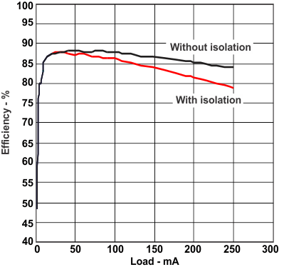
TPS61093 eff_ld_lvs992.gifFigure 8. Efficiency vs Load