SLVSA18A September 2009 – July 2015 TPS61161-Q1
PRODUCTION DATA.
- 1 Features
- 2 Applications
- 3 Description
- 4 Revision History
- 5 Pin Configuration and Functions
- 6 Specifications
- 7 Detailed Description
- 8 Applications and Implementation
- 9 Power Supply Recommendations
- 10Layout
- 11Device and Documentation Support
- 12Mechanical, Packaging, and Orderable Information
8 Applications and Implementation
NOTE
Information in the following applications sections is not part of the TI component specification, and TI does not warrant its accuracy or completeness. TI’s customers are responsible for determining suitability of components for their purposes. Customers should validate and test their design implementation to confirm system functionality.
8.1 Application Information
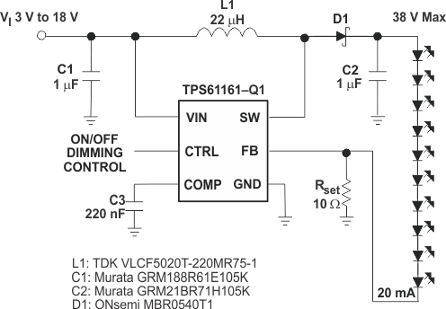
In the application, TPS61161-Q1 drives 10 LEDs, the output current is set at 20mA, the circuit can support wide range input voltage from 3 V to 18 V. By applying PWM signal on CTRL pin, the circuit can realize PWM dimming control.
8.2 Typical Application
 Figure 15. LED Drivers With 10 White LEDs Schematic
8.2.1 Design Requirements
Table 4 lists the input parameters for this design example.
Table 4. Design Parameters
| PARAMETER | EXAMPLE VALUE |
|---|---|
| Brightness control | PWM Dimming |
| Input voltage | 3 V to 18 V |
| Output current | 20 mA |
| LED loads | 10 LEDs |
8.2.2 Detailed Design Procedure
8.2.2.1 Current Program
The FB voltage is regulated by a low 0.2-V reference voltage. The LED current is programmed externally using a current-sense resistor in series with the LED string. The value of the RSET is calculated using Equation 2:

where
- ILED = output current of LEDs
- VFB = regulated voltage of FB
- RSET = current sense resistor
The output current tolerance depends on the FB accuracy and the current sensor resistor accuracy.
8.2.2.2 Maximum Output Current
The overcurrent limit in a boost converter limits the maximum input current and thus maximum input power for a given input voltage. Maximum output power is less than maximum input power due to power conversion losses. Therefore, the current limit setting, input voltage, output voltage and efficiency can all change maximum current output. The current limit clamps the peak inductor current; therefore, the ripple must be subtracted to derive maximum dc current. The ripple current is a function of switching frequency, inductor value and duty cycle. The following equations take into account of all of the previous factors for maximum output current calculation.

where
- IP = inductor peak to peak ripple
- L = inductor value
- VF = Schottky diode forward voltage
- FS = switching frequency
- VOUT = output voltage of the boost converter. It is equal to the sum of VFB and the voltage drop across LEDs.

where
- IOUT_MAX = maximum output current of the boost converter
- ILIM = overcurrent limit
- η = efficiency
For instance, when VIN is 3 V, 8 LEDs output equivalent to VOUT of 26 V, the inductor is 22 µH, the Schottky forward voltage is 0.2 V; and then the maximum output current is 65 mA in typical condition. When VIN is 5 V, 10 LEDs output equivalent to VOUT of 32 V, the inductor is 22 µH, the Schottky forward voltage is 0.2 V; and then the maximum output current is 85 mA in typical condition.
8.2.2.3 Inductor Selection
The selection of the inductor affects steady state operation as well as transient behavior and loop stability. These factors make it the most important component in power regulator design. There are three important inductor specifications, inductor value, dc resistance and saturation current. Considering inductor value alone is not enough.
The inductor value determines the inductor ripple current. Choose an inductor that can handle the necessary peak current without saturating, according to half of the peak-to-peak ripple current given by Equation 3, pause the inductor dc current given by:

Inductor values can have ±20% tolerance with no current bias. When the inductor current approaches saturation level, its inductance can decrease 20% to 35% from the 0-A value depending on how the inductor vendor defines saturation current. Using an inductor with a smaller inductance value forces discontinuous PWM when the inductor current ramps down to zero before the end of each switching cycle. This reduces the boost converter’s maximum output current, causes large input voltage ripple and reduces efficiency. Large inductance value provides much more output current and higher conversion efficiency. For these reasons, TI recommends a 10-µH to 22-µH inductor value range. A 22-µH inductor optimized the efficiency for most application while maintaining low inductor peak to peak ripple. Table 5 lists the recommended inductor for the TPS61161-Q1. When recommending inductor value, the factory has considered –40% and 20% tolerance from its nominal value.
TPS61161-Q1 has built-in slope compensation to avoid sub-harmonic oscillation associated with current mode control. If the inductor value is lower than 10 µH, the slope compensation may not be adequate, and the loop can be unstable. Therefore, customers must verify the inductor in their application if it is different from the recommended values.
Table 5. Recommended Inductors for TPS61161-Q1
| PART NUMBER | L (µH) |
DCR MAX (Ω) |
SATURATION CURRENT (mA) |
SIZE (L × W × H mm) |
VENDOR |
|---|---|---|---|---|---|
| LQH3NPN100NM0 | 10 | 0.3 | 750 | 3×3×1.5 | Murata |
| VLCF5020T-220MR75-1 | 22 | 0.4 | 750 | 5×5×2 | TDK |
| CDH3809/SLD | 10 | 0.3 | 570 | 4×4×1 | Sumida |
| A997AS-220M | 22 | 0.4 | 510 | 4×4×1.8 | TOKO |
8.2.2.4 Schottky Diode Selection
The high switching frequency of the TPS61161-Q1 demands a high-speed rectification for optimum efficiency. Ensure that the diode average and peak current rating exceeds the average output current and peak inductor current. In addition, the diode’s reverse breakdown voltage must exceed the open LED protection voltage. The ONSemi MBR0540 and the ZETEX ZHCS400 are recommended for TPS61161-Q1.
8.2.2.5 Compensation Capacitor Selection
The compensation capacitor C3 (see the block diagram), connected from COMP pin to GND, is used to stabilize the feedback loop of the TPS61161-Q1. Use a 220-nF ceramic capacitor for C3.
8.2.2.6 Input and Output Capacitor Selection
The output capacitor is mainly selected to meet the requirements for the output ripple and loop stability. This ripple voltage is related to the capacitor’s capacitance and its equivalent series resistance (ESR). Assuming a capacitor with zero ESR, the minimum capacitance needed for a given ripple can be calculated by

where
- VRIPPLE = peak-to-peak output ripple.
The additional output ripple component caused by ESR is calculated using:

Due to its low ESR, Vripple_ESR can be neglected for ceramic capacitors, but must be considered if tantalum or electrolytic capacitors are used.
Take care when evaluating a ceramic capacitor’s derating under dc bias, aging, and ac signal. For example, larger form factor capacitors (in 1206 size) have a resonant frequencies in the range of the switching frequency. So the effective capacitance is significantly lower. The dc bias can also significantly reduce capacitance. Ceramic capacitors can loss as much as 50% of its capacitance at its rated voltage. Therefore, leave the margin on the voltage rating to ensure adequate capacitance at the required output voltage.
TI recommends the capacitor in the range of 1 µF to 4.7 µF for input side. The output requires a capacitor in the range of 0.47 µF to 10 µF. The output capacitor affects the loop stability of the boost regulator. If the output capacitor is below the range, the boost regulator can potentially become unstable. For example, if use the output capacitor of 0.1 µF, a 470 nF compensation capacitor must be used for the loop stable.
The popular vendors for high value ceramic capacitors are:
TDK (http://www.component.tdk.com/components.php)
Murata (http://www.murata.com/cap/index.html)
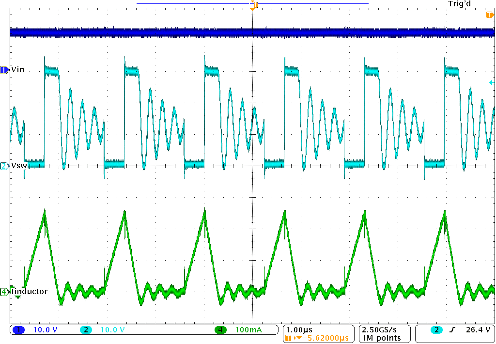
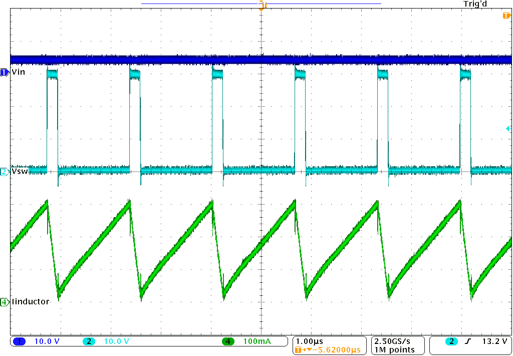
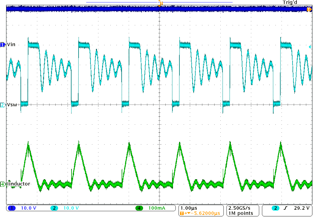
8.2.3 Application Curves


