ZHCSJH2E November 2007 – April 2019 TPS61165
PRODUCTION DATA.
- 1 特性
- 2 应用
- 3 说明
- 4 修订历史记录
- 5 Device Options
- 6 Pin Configuration and Functions
- 7 Specifications
- 8 Detailed Description
- 9 Application and Implementation
- 10Power Supply Recommendations
- 11Layout
- 12器件和文档支持
- 13机械、封装和可订购信息
封装选项
机械数据 (封装 | 引脚)
散热焊盘机械数据 (封装 | 引脚)
- DRV|6
订购信息
9.2.1.2.2 PWM Brightness Dimming
When the CTRL pin is constantly high, the FB voltage is regulated to 200 mV typically. However, the CTRL pin allows a PWM signal to reduce this regulation voltage; therefore, it achieves LED brightness dimming. The relationship between the duty cycle and FB voltage is shown in Equation 6.
where
- Duty = duty cycle of the PWM signal
- 200 mV = internal reference voltage
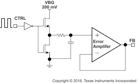
As shown in Figure 10, the device chops up the internal 200-mV reference voltage at the duty cycle of the PWM signal. The pulse signal is then filtered by an internal low pass filter. The output of the filter is connected to the error amplifier as the reference voltage for the FB pin regulation. Therefore, although a PWM signal is used for brightness dimming, only the WLED DC current is modulated, which is often referred as analog dimming. This eliminates the audible noise which often occurs when the LED current is pulsed in replica of the frequency and duty cycle of PWM control. Unlike other methods which filters the PWM signal for analog dimming, TPS61165 regulation voltage is independent of the PWM logic voltage level which often has large variations.
For optimum performance, use the PWM dimming frequency in the range of 6.5 kHz to 100 kHz. The requirement of minimum dimming frequency comes from the EasyScale detection delay and detection time specification in the dimming mode selection. Because the CTRL pin is logic only pin, adding an external RC filter applied to the pin does not work.
To use lower PWM dimming, add external RC network connected to the FB pin as shown in Additional Application Circuits.
