ZHCSD24B October 2014 – June 2024 TPS61169
PRODUCTION DATA
- 1
- 1 特性
- 2 应用
- 3 说明
- 4 Pin Configuration and Functions
- 5 Specifications
- 6 Detailed Description
- 7 Application and Implementation
- 8 Device and Documentation Support
- 9 Revision History
- 10Mechanical, Packaging, and Orderable Information
6.3.5 LED Brightness Dimming
The TPS61169 receives PWM dimming signal at CTRL pin to control the total output current. When the CTRL pin is constantly high, the FB voltage is regulated to 204mV typically. When the duty cycle of the input PWM signal is low, the regulation voltage at FB pin is reduced, and the total output current is reduced; therefore, it achieves LED brightness dimming. The relationship between the duty cycle and FB regulation voltage is given by:

where
- Duty = Duty cycle of the PWM signal
- 204mV = internal reference voltage
Thus, the user can easily control the WLED brightness by controlling the duty cycle of the PWM signal.
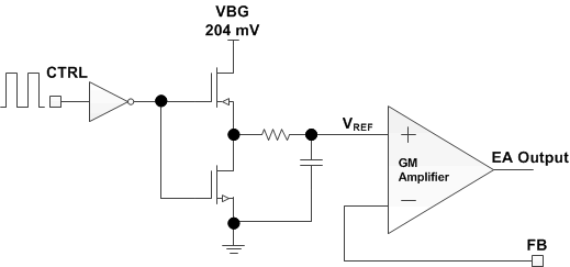
As shown in Figure 6-1, the device chops up the internal 204mV reference voltage at the duty cycle of the PWM signal. The pulse signal is then filtered by an internal low-pass filter. The output of the filter is connected to the GM amplifier as the reference voltage for the FB pin regulation. Therefore, although a PWM signal is used for brightness dimming, only the WLED DC current is modulated, which is often referred as analog dimming. This eliminates the audible noise which often occurs when the LED current is pulsed in replica of the frequency and duty cycle of PWM control. Unlike other methods which filter the PWM signal for analog dimming, TPS61169 regulation voltage is independent of the PWM logic voltage level which often has large variations.
For optimum performance, use the PWM dimming frequency in the range of 5kHz to 100kHz. If the PWM frequency is lower than 5kHz, it is out of the low pass filter's filter range, the FB regulation voltage ripple becomes large, causing large output ripple and may generate audible noise.
 Figure 6-1 Programmable FB Voltage Using PWM Signal