ZHCSD24B October   2014  – June 2024 TPS61169

PRODUCTION DATA  

  1.   1
  2. 特性
  3. 应用
  4. 说明
  5. Pin Configuration and Functions
  6. Specifications
    1. 5.1 Absolute Maximum Ratings
    2. 5.2 ESD Ratings
    3. 5.3 Recommended Operating Conditions
    4. 5.4 Thermal Information
    5. 5.5 Electrical Characteristics
    6. 5.6 Typical Characteristics
  7. Detailed Description
    1. 6.1 Overview
    2. 6.2 Functional Block Diagram
    3. 6.3 Feature Description
      1. 6.3.1 Soft Start-Up
      2. 6.3.2 Open LED Protection
      3. 6.3.3 Shutdown
      4. 6.3.4 Current Program
      5. 6.3.5 LED Brightness Dimming
      6. 6.3.6 Undervoltage Lockout
      7. 6.3.7 Thermal Foldback and Thermal Shutdown
    4. 6.4 Device Functional Modes
      1. 6.4.1 Operation With CTRL
  8. Application and Implementation
    1. 7.1 Application Information
    2. 7.2 Typical Application
      1. 7.2.1 Design Requirements
      2. 7.2.2 Detailed Design Procedure
        1. 7.2.2.1 Inductor Selection
        2. 7.2.2.2 Schottky Diode Selection
        3. 7.2.2.3 Output Capacitor Selection
        4. 7.2.2.4 LED Current Set Resistor
        5. 7.2.2.5 Thermal Considerations
    3. 7.3 Application Curves
    4. 7.4 Power Supply Recommendations
    5. 7.5 Layout
      1. 7.5.1 Layout Guidelines
      2. 7.5.2 Layout Example
  9. Device and Documentation Support
    1. 8.1 Device Support
    2. 8.2 接收文档更新通知
    3. 8.3 支持资源
    4. 8.4 Trademarks
    5. 8.5 静电放电警告
    6. 8.6 术语表
  10. Revision History
  11. 10Mechanical, Packaging, and Orderable Information

封装选项

机械数据 (封装 | 引脚)
散热焊盘机械数据 (封装 | 引脚)
订购信息

Pin Configuration and Functions

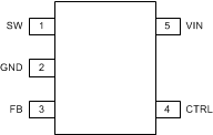
TPS61169 DCK Package5-Pin SC70(Top View)Figure 4-1 DCK Package5-Pin SC70(Top View)
Table 4-1 Pin Functions
PIN I/O DESCRIPTION
NUMBER NAME
1 SW I Drain connection of the internal power FET.
2 GND O Ground
3 FB I Feedback pin for current. Connect the sense resistor from FB to GND.
4 CTRL I PWM dimming signal input
5 VIN I Supply input pin