ZHCSJF8F December 2008 – April 2019 TPS61175
PRODUCTION DATA.
- 1 特性
- 2 应用
- 3 说明
- 4 修订历史记录
- 5 Pin Configuration and Functions
- 6 Specifications
- 7 Detailed Description
-
8 Application and Implementation
- 8.1 Application Information
- 8.2
Typical Application
- 8.2.1 Design Requirements
- 8.2.2
Detailed Design Procedure
- 8.2.2.1 Custom Design with WEBENCH Tools
- 8.2.2.2 Determining the Duty Cycle
- 8.2.2.3 Selecting the Inductor
- 8.2.2.4 Computing the Maximum Output Current
- 8.2.2.5 Setting Output Voltage
- 8.2.2.6 Setting the Switching Frequency
- 8.2.2.7 Setting the Soft-Start Time
- 8.2.2.8 Selecting the Schottky Diode
- 8.2.2.9 Selecting the Input and Output Capacitors
- 8.2.2.10 Compensating the Small Signal Control Loop
- 8.2.3 Application Curves
- 9 Power Supply Recommendations
- 10Layout
- 11器件和文档支持
- 12机械、封装和可订购信息
6.6 Typical Characteristics
Circuit of Figure 1; L1 = D104C2-10μH; D1 = SS3P6L-E3/86A, R4 = 80kΩ, R3 = 10kΩ, C4 = 22nF,C2 = 10μF;VIN = 5V, VOUT = 24V, IOUT = 200mA (unless otherwise noted)
Table 1. Table Of Graphs
| FIGURE | ||
|---|---|---|
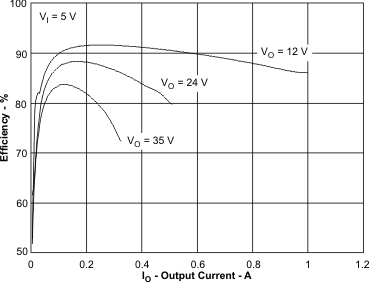
| Efficiency | VIN = 5 V, VOUT = 12 V, 24 V, 35 V | Figure 1 |
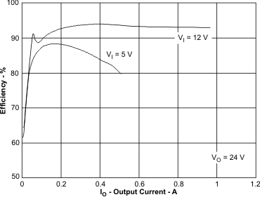
| Efficiency | VIN = 5 V, 12 V; VOUT = 24 V | Figure 2 |
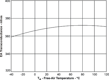
| Error amplifier transconductance | vs Temperature | Figure 3 |
| Switch current limit | vs Temperature | Figure 4 |
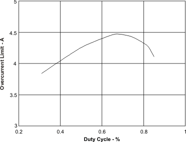
| Switch current limit | vs Duty cycle | Figure 5 |
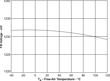
| FB accuracy | vs Temperature | Figure 6 |
| Line transient response | VIN = 4.5 V to 5 V | Figure 12 |
| Load transient response | IOUT = 100 mA to 300 mA; refer to 'compensating the control loop' for optimization | Figure 13 |
| PWM Operation | Figure 14 | |
| Pulse skipping | No load | Figure 15 |
| Start-up | C3 = 47 nF | Figure 16 |
