ZHCSDK2B March 2015 – March 2017 TPS61177A
PRODUCTION DATA.
- 1 特性
- 2 应用范围
- 3 说明
- 4 修订历史记录
- 5 Pin Configuration and Functions
- 6 Specifications
-
7 Detailed Description
- 7.1 Overview
- 7.2 Functional Block Diagram
- 7.3
Feature Description
- 7.3.1 Supply Voltage
- 7.3.2 Boost Regulator
- 7.3.3 Programmable Switch Frequency and Slew Rate
- 7.3.4 LED Current Sinks
- 7.3.5 Enable and Start-Up Timing
- 7.3.6 Input Undervoltage Protection (UVLO)
- 7.3.7 Overvoltage Protection (OVP)
- 7.3.8 Current-Sink Open Protection
- 7.3.9 Overcurrent Protection
- 7.3.10 Thermal Protection
- 7.4 Device Functional Modes
- 7.5 Programming
- 7.6
Register Maps
- 7.6.1 MODE (A0h)
- 7.6.2 CS (A1h)
- 7.6.3 UVLO (A2h)
- 7.6.4 FREQ (A3h)
- 7.6.5 SR (A4h)
- 7.6.6 ILIM (A5h)
- 7.6.7 Control (FFh)
- 7.6.8 Example - Writing to a Single RAM Register
- 7.6.9 Example - Writing to Multiple RAM Registers
- 7.6.10 Example - Saving Contents of all RAM Registers to E2PROM
- 7.6.11 Example - Reading from a Single RAM Register
- 7.6.12 Example - Reading from a Single E2PROM Register
- 7.6.13 Example - Reading from Multiple RAM Registers
- 7.6.14 Example - Reading from Multiple E2PROM Registers
- 8 Application and Implementation
- 9 Power Supply Recommendations
- 10Layout
- 11器件和文档支持
- 12机械、封装和可订购信息
10 Layout
10.1 Layout Guidelines
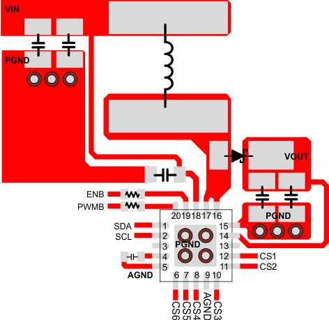
As for all switching power supplies, especially those providing high current and using high switching frequencies, layout is an important design step. If layout is not carefully done, the regulator could show instability as well as EMI problems. Therefore, use wide and short traces for high current paths. The input capacitor, C1 in the Typical Application, must not only to be close to the VIN pin, but also to the GND pin in order to reduce the input ripple seen by the device. The input capacitor, C4 in the Typical Application, must also be placed close to the inductor. C5 is the reference capacitor for the internal integration circuit. It must be placed as close between the REF and AGND pins as possible to prevent any noise insertion to the digital circuits. The LX pin carries high current with fast rising and falling edges. Therefore, the connection between the pin to the inductor and Schottky diode must be kept as short and wide as possible. It is also beneficial to have the ground of the output capacitor C2 close to the PGND pin because there is a large ground return current flowing between them. When laying out signal grounds, TI recommends using short traces separated from power ground traces, and connecting them together at a single point, for example on the DAP. The DAP must be soldered on to the PCB and connected to the GND pin of the device. An additional thermal via can significantly improve power dissipation of the device.
10.2 Layout Example
