ZHCSG87E February 2017 – August 2019 TPS61178
PRODUCTION DATA.
- 1 特性
- 2 应用
- 3 说明
- 4 修订历史记录
- 5 Device Comparison Table
- 6 Pin Configuration and Functions
- 7 Specifications
-
8 Detailed Description
- 8.1 Overview
- 8.2 Functional Block Diagram
- 8.3
Feature Description
- 8.3.1 Under-voltage Lockout
- 8.3.2 Enable and Disable
- 8.3.3 Startup
- 8.3.4 Load Disconnect Gate Driver
- 8.3.5 Adjustable Peak Current Limit
- 8.3.6 Output Short Protection (with load disconnected FET)
- 8.3.7 Adjustable Switching Frequency
- 8.3.8 External Clock Synchronization (TPS611781)
- 8.3.9 Error Amplifier
- 8.3.10 Slope Compensation
- 8.3.11 Start-up with the Output Pre-Biased
- 8.3.12 Bootstrap Voltage (BST)
- 8.3.13 Over-voltage Protection
- 8.3.14 Thermal Shutdown
- 8.4 Device Functional Modes
-
9 Application and Implementation
- 9.1 Application Information
- 9.2
Typical Application
- 9.2.1 Design Requirements
- 9.2.2 Detailed Design Procedure
- 9.2.3 Setting the Current Limit
- 9.2.4 Setting the Output Voltage
- 9.2.5 TPS61178 Application Waveform
- 9.3 System Examples
- 10Power Supply Recommendations
- 11Layout
- 12器件和文档支持
- 13机械、封装和可订购信息
9.2.4.4.1 Small Signal Model
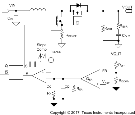
The TPS61178x uses the fixed frequency peak current mode control; there is an internal adaptive slope compensation to avoid the sub-harmonic oscillation. With the inductor current information sensed, the small-signal model of the power stage reduces from a two-pole system, created by L and COUT, to a single-pole system, created by ROUT and COUT. The single-pole system is easily used with the loop compensation. Figure 24 shows the equivalent small signal elements of a boost converter.
 Figure 24. TPS61178x Control Equivalent Circuitry Model
 The small signal of power stage including the slope compensation is:

where
- D is the duty cycle
- ROUT is the output load resistor
- RSENSE is the equivalent internal current sense resistor, which is typically 0.083 Ω of TPS61178x
The single pole of the power stage is:

where
- COUT is the output capacitance, for a boost converter having multiple, identical output capacitors in parallel, simply combine the capacitors with the equivalent capacitance
The zero created by the ESR of the output capacitor is:

where
- RESR is the equivalent resistance in series of the output capacitor.
The right-hand plane zero is:

where
- D is the duty cycle
- ROUT is the output load resistor
- L is the inductance
Using He(s) to model the inductor current sampling effect as well as the slope compensation effect on the small signal response, is shown in Equation 19


where
- Sn is the slew rate of the inductor current ramping up

where
- Se is the slope compensation slew rate
- Rdson_LS is the on resistance of Low-side FET
The slope compensation adaptively changes with the switching frequency and duty cycle.
He(s) models the inductor current sampling effect as well as the slope compensation effect on the small signal response. Note that if Sn > Se, e.g., when L is too small, the converter operates as a voltage mode converter and the above model no longer holds.
The TPS61178x COMP pin is the output of the internal trans-conductance amplifier.
Equation 22 shows the equation for feedback resistor network and the error amplifier.

where
- kCOMP and REA are the ratio of peak current / comp voltage, for TPS61178x, the typical value is kCOMP = 12 A / V and REA = 20 MΩ.
- ƒP1, ƒP2 is the pole's frequency of the compensation, fZ is the zero’s frequency of the compensation network. network

where
- CC is the zero capacitor compensation

where
- CP is the pole capacitor compensation
- RC is the resistor of the compensation network
