ZHCS002E March 2007 – December 2014 TPS61200 , TPS61201 , TPS61202
PRODUCTION DATA.
- 1 特性
- 2 应用范围
- 3 说明
- 4 典型应用
- 5 修订历史记录
- 6 Device Options
- 7 Pin Configuration and Functions
- 8 Specifications
- 9 Parameter Measurement Information
- 10Detailed Description
- 11Application and Implementation
- 12Power Supply Recommendations
- 13Layout
- 14器件和文档支持
- 15机械、封装和可订购信息
11 Application and Implementation
NOTE
Information in the following applications sections is not part of the TI component specification, and TI does not warrant its accuracy or completeness. TI’s customers are responsible for determining suitability of components for their purposes. Customers should validate and test their design implementation to confirm system functionality.
11.1 Application Information
The TPS6120x DC-DC converters are intended for systems powered by a single up to triple cell Alkaline, NiCd, NiMH battery with a typical terminal voltage between 0.7 V and 5.5 V. They can also be used in systems powered by one-cell Li-Ion or Li-Polymer with a typical voltage between 2.5 V and 4.2 V. Additionally, any other voltage source like solar cells or fuel cells with a typical output voltage between 0.3 V and 5.5 V can power systems where the TPS6120x is used.
11.2 Typical Application
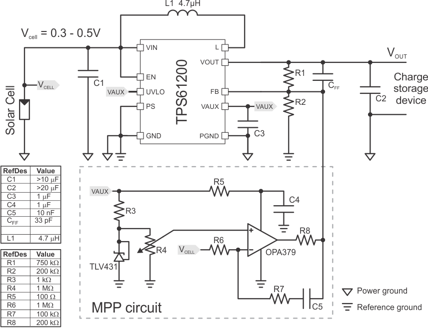
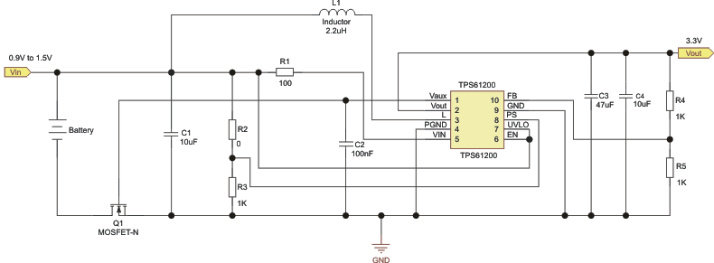
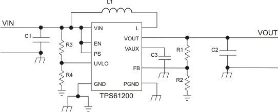 Figure 15. Typical Application Circuit for Adjustable Output Voltage Option
11.2.1 Design Requirements
In this example, TPS61200 is used to design a 3.3-V power supply with 100-mA output current capability. The TPS61200 can be powered by either a single-cell, two-cell, or three-cell alkaline, NiCd or NiMH, or one-cell Li-Ion or Li-Polymer battery. In this example, the input voltage range is from 0.8 V to 1.65 V for single-cell alkaline input.
11.2.2 Detailed Design Procedure
Table 2. List of Components
| COMPONENT REFERENCE | PART NUMBER | MANUFACTURER | VALUE |
|---|---|---|---|
| C1 | any | 10 μF, X7R Ceramic | |
| C2 | any | 2 x 10 μF, X7R Ceramic | |
| C3 | any | 1 µF, X7R, Ceramic | |
| L1 | LPS3015-222ML | Coilcraft | 2.2 μH |
11.2.2.1 Programming the Output Voltage
Within the TPS6120X family, there are fixed and adjustable output voltage versions available. To properly configure the fixed output voltage devices, the FB pin is used to sense the output voltage. This means that it must be connected directly to VOUT. For the adjustable output voltage version, an external resistor divider is used to adjust the output voltage. The resistor divider must be connected between VOUT, FB and GND. When the output voltage is regulated properly, the typical value of the voltage at the FB pin is 500 mV. The maximum recommended value for the output voltage is 5.5 V. The current through the resistive divider should be about 100 times greater than the current into the FB pin. The typical current into the FB pin is 0.01 μA, and the voltage across the resistor between FB and GND, R2, is typically 500 mV. Based on those two values, the recommended value for R2 should be lower than 500 kΩ, in order to set the divider current at 1 μA or higher. It is recommended to keep the value for this resistor in the range of 200 kΩ. The value of the resistor connected between VOUT and FB, R1, depending on the needed output voltage (VOUT), can be calculated using Equation 1:

As an example, for an output voltage of 3.3 V, a 1-MΩ resistor should be chosen for R1 when a 180-kΩ is selected for R2.
11.2.2.2 Programming the UVLO Threshold Voltage
The UVLO input can be used to shut down the main output if the supply voltage is getting too low. The internal reference threshold is typically 250 mV. If the supply voltage should cause the shutdown when it is dropping below 250 mV, VIN can be connected directly to the UVLO pin. If the shutdown should happen at higher voltages, a resistor divider can be used. R3 and R4 in Figure 15 show an example of how to monitor the input voltage of the circuit. The current through the resistive divider should be about 100 times greater than the current into the UVLO pin. The typical current into the UVLO pin is 0.01 μA, and the voltage across R4 is equal to the UVLO voltage threshold that is generated on-chip, which has a value of 250 mV. Therefore, the recommended value for R4 is in the range of 250 kΩ. From this, the value of resistor R3, depending on the desired shutdown voltage VINMIN, can be calculated using Equation 2.

11.2.2.3 Inductor Selection
To make sure that the TPS6120X devices can operate, an inductor must be connected between the VIN and L pins. To estimate the minimum inductance value, Equation 3 can be used.

In Equation 3, the minimum inductance, LMIN , for boost mode operation is calculated. VIN is the maximum input voltage. The recommended inductor value range is between 1.5 μH and 4.7 μH. The minimum inductor value should not be below 1.5 μH, even if Equation 3 yields something lower. Using 2.2 μH is recommended anyway for getting best performance over the whole input and output voltage range.
With the chosen inductance value, the peak current for the inductor in steady state operation can be calculated using Equation 4.

This would be the critical value for the current rating for selecting the inductor. It also needs to be taken into account that load transients and error conditions may cause higher inductor currents. The following inductor series from different suppliers have been used with TPS6120x converters:
Table 3. List of Inductors
| VENDOR | INDUCTOR SERIES |
|---|---|
| Coilcraft | LPS3015 |
| LPS4012 | |
| Murata | LQH3NP |
| Tajo Yuden | NR3015 |
| Wurth Elektronik | WE-TPC Typ S |
11.2.2.4 Capacitor Selection
11.2.2.4.1 Input Capacitor
At least a 4.7-μF input capacitor is recommended to improve transient behavior of the regulator and EMI behavior of the total power supply circuit. An X5R or X7R ceramic capacitor placed as close as possible to the VIN and PGND pins of the IC is recommended.
An R-C filter may be placed on the VIN pin to improve performance in applications with a noisy input source. A 100-Ω resistor and 0.1-µF capacitor are recommended in this case. This filter is not required operation.
11.2.2.4.2 Output Capacitor
For the output capacitor, it is recommended to use small X5R or X7R ceramic capacitors placed as close as possible to the VOUT and PGND pins of the IC. If, for any reason, the application requires the use of large capacitors which can not be placed close to the IC, using a smaller ceramic capacitor in parallel to the large one is required. This small capacitor should be placed as close as possible to the VOUT and PGND pins of the IC.
To get an estimate of the recommended minimum output capacitance, Equation 5 can be used.

A capacitor with a value in the range of the calculated minimum should be used. This is required to maintain control loop stability. There are no additional requirements regarding minimum ESR. There is also no upper limit for the output capacitance value. Larger capacitors cause lower output voltage ripple as well as lower output voltage drops during load transients.
11.2.2.4.3 Capacitor at VAUX
Between the VAUX pin and GND pin, a capacitor must be connected. This capacitor is used to maintain and filter the control supply voltage, which is chosen from the highest of VIN, VOUT, and L. It is charged during startup and before the main output VOUT is turned on. To ensure stable operation, using at least 0.1μF is recommended. At output voltages below 2.5 V, the capacitance should be in the range of 1 μF. Since this capacitor is also used as a snubber capacitor for the main switch, using a X5R or X7R ceramic capacitor with low ESR is important.
11.2.3 Application Curves
| FIGURE | |
|---|---|
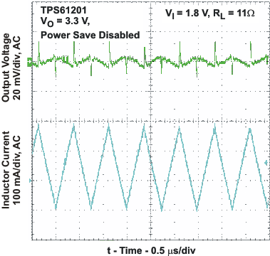
| Output Voltage TPS61201, Power Save Mode Disabled | Figure 16 |
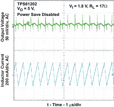
| Output Voltage TPS61202, Power Save Mode Disabled | Figure 17 |
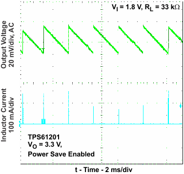
| Output Voltage TPS61201, Power Save Mode Enabled | Figure 18 |
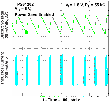
| Output Voltage TPS61202, Power Save Mode Enabled | Figure 19 |
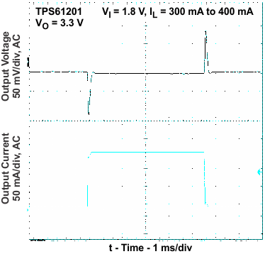
| TPS61201 Load Transient Response | Figure 20 |
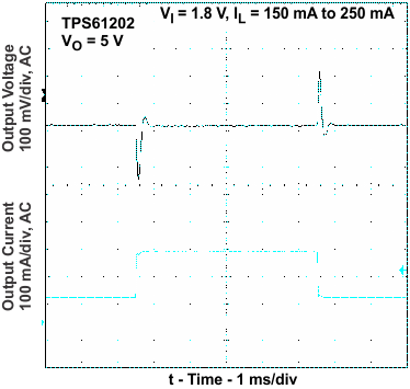
| TPS61202 Load Transient Response | Figure 21 |
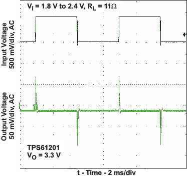
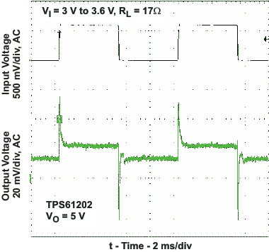
| TPS61201 Line Transient Response | Figure 22 |
| TPS61202 Line Transient Response | Figure 23 |
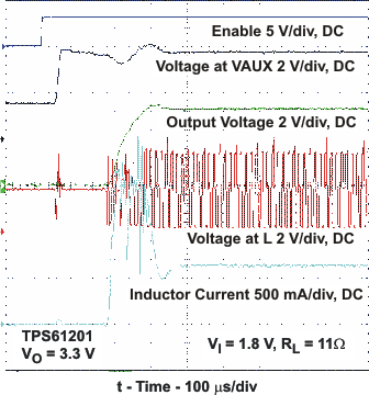
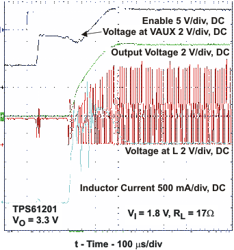
| TPS61201 Startup after Enable | Figure 24 |
| TPS61202 Startup after Enable | Figure 25 |
