ZHCSFD9B July   2016  – October 2018 TPS61230A

PRODUCTION DATA.  

  1. 特性
  2. 应用
  3. 说明
    1.     Device Images
      1.      典型应用
      2.      效率
  4. 修订历史记录
  5. Pin Configuration and Functions
    1.     Pin Functions
  6. Specifications
    1. 6.1 Absolute Maximum Ratings
    2. 6.2 ESD Ratings
    3. 6.3 Recommended Operating Conditions
    4. 6.4 Thermal Information
    5. 6.5 Electrical Characteristics
    6. 6.6 Typical Characteristics
  7. Detailed Description
    1. 7.1 Overview
    2. 7.2 Functional Block Diagram
    3. 7.3 Feature Description
      1. 7.3.1 Startup
      2. 7.3.2 Enable and Disable
      3. 7.3.3 Under-Voltage Lockout (UVLO)
      4. 7.3.4 Current Limit Operation
      5. 7.3.5 Over Voltage Protection
      6. 7.3.6 Load Disconnect
      7. 7.3.7 Thermal Shutdown
    4. 7.4 Device Functional Modes
      1. 7.4.1 PWM Mode
      2. 7.4.2 PFM Mode
  8. Application and Implementation
    1. 8.1 Application Information
    2. 8.2 Typical Applications
      1. 8.2.1 TPS61230A 2.5-V to 4.5-V Input, 5-V Output Converter
        1. 8.2.1.1 TPS61230A 5-V Output Design Requirements
        2. 8.2.1.2 TPS61230A 5-V Detailed Design Procedure
          1. 8.2.1.2.1 Programming The Output Voltage
          2. 8.2.1.2.2 Inductor and Capacitor Selection
            1. 8.2.1.2.2.1 Inductor Selection
            2. 8.2.1.2.2.2 Output Capacitor Selection
            3. 8.2.1.2.2.3 Input Capacitor Selection
          3. 8.2.1.2.3 Loop Stability, Feed Forward Capacitor
        3. 8.2.1.3 TPS61230A 5-V Output Application Performance Plots
      2. 8.2.2 Systems Example - TPS61230A with Feed Forward Capacitor for Best Transient Response
  9. Power Supply Recommendations
  10. 10Layout
    1. 10.1 Layout Guidelines
    2. 10.2 Layout Example
    3. 10.3 Thermal Considerations
  11. 11器件和文档支持
    1. 11.1 器件支持
      1. 11.1.1 第三方米6体育平台手机版_好二三四免责声明
    2. 11.2 文档支持
      1. 11.2.1 相关文档
    3. 11.3 接收文档更新通知
    4. 11.4 社区资源
    5. 11.5 商标
    6. 11.6 静电放电警告
    7. 11.7 术语表
  12. 12机械、封装和可订购信息

封装选项

机械数据 (封装 | 引脚)
散热焊盘机械数据 (封装 | 引脚)
订购信息

Typical Characteristics

VIN = 3.6 V, VOUT = 5.0 V, TJ = -40°C to 125 °C, unless otherwise noted.
TPS61230A D009_SLVSCZ5.gif
TA = 25 ºC
Figure 1. Efficiency vs. Output Current
TPS61230A D015_SLVSCZ5.gif
TA = 25 ºC
Figure 3. Line Regulation
TPS61230A D013_SLVSCZ5.gif
TA = 25 ºC
Figure 5. Frequency vs. Load
TPS61230A D002_SLVSCZ5.gif
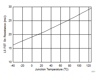
VOUT = 5 V VIN = 3.6V
Figure 7. Low-Side FET Rdson vs Junction Temperature
TPS61230A D017_SLVSCZ5.gif
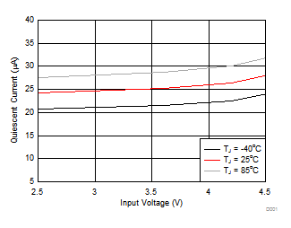
Figure 9. Quiescent Current vs Input Voltage
TPS61230A D007_SLVSCZ5.gif
Figure 11. Vin UVLO Threshold vs Junction Temperature
TPS61230A D010_SLVSCZ5.gif
TA = 25 ºC
Figure 2. Efficiency vs. Input Voltage
TPS61230A D012_SLVSCZ5.gif
TA = 25 ºC
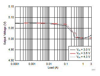
Figure 4. Load Regulation
TPS61230A D001_SLVSCZ5.gif
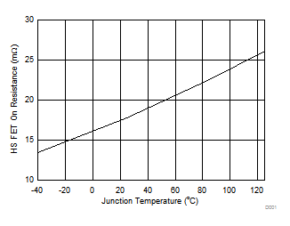
VOUT = 5 V VIN = 3.6V
Figure 6. High-Side FET Rdson vs Junction Temperature
TPS61230A D003_SLVSCZ5.gif
Figure 8. Voltage Reference vs Junction Temperature
TPS61230A D016_SLVSCZ5.gif
Figure 10. Switch Valley Current Limit vs Input Voltage
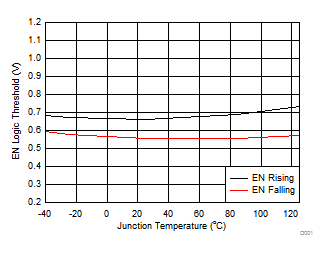
TPS61230A D008_SLVSCZ5.gif
Figure 12. EN logic Threshold vs Junction Temperature