ZHCSFD9B July   2016  – October 2018 TPS61230A

PRODUCTION DATA.  

  1. 特性
  2. 应用
  3. 说明
    1.     Device Images
      1.      典型应用
      2.      效率
  4. 修订历史记录
  5. Pin Configuration and Functions
    1.     Pin Functions
  6. Specifications
    1. 6.1 Absolute Maximum Ratings
    2. 6.2 ESD Ratings
    3. 6.3 Recommended Operating Conditions
    4. 6.4 Thermal Information
    5. 6.5 Electrical Characteristics
    6. 6.6 Typical Characteristics
  7. Detailed Description
    1. 7.1 Overview
    2. 7.2 Functional Block Diagram
    3. 7.3 Feature Description
      1. 7.3.1 Startup
      2. 7.3.2 Enable and Disable
      3. 7.3.3 Under-Voltage Lockout (UVLO)
      4. 7.3.4 Current Limit Operation
      5. 7.3.5 Over Voltage Protection
      6. 7.3.6 Load Disconnect
      7. 7.3.7 Thermal Shutdown
    4. 7.4 Device Functional Modes
      1. 7.4.1 PWM Mode
      2. 7.4.2 PFM Mode
  8. Application and Implementation
    1. 8.1 Application Information
    2. 8.2 Typical Applications
      1. 8.2.1 TPS61230A 2.5-V to 4.5-V Input, 5-V Output Converter
        1. 8.2.1.1 TPS61230A 5-V Output Design Requirements
        2. 8.2.1.2 TPS61230A 5-V Detailed Design Procedure
          1. 8.2.1.2.1 Programming The Output Voltage
          2. 8.2.1.2.2 Inductor and Capacitor Selection
            1. 8.2.1.2.2.1 Inductor Selection
            2. 8.2.1.2.2.2 Output Capacitor Selection
            3. 8.2.1.2.2.3 Input Capacitor Selection
          3. 8.2.1.2.3 Loop Stability, Feed Forward Capacitor
        3. 8.2.1.3 TPS61230A 5-V Output Application Performance Plots
      2. 8.2.2 Systems Example - TPS61230A with Feed Forward Capacitor for Best Transient Response
  9. Power Supply Recommendations
  10. 10Layout
    1. 10.1 Layout Guidelines
    2. 10.2 Layout Example
    3. 10.3 Thermal Considerations
  11. 11器件和文档支持
    1. 11.1 器件支持
      1. 11.1.1 第三方米6体育平台手机版_好二三四免责声明
    2. 11.2 文档支持
      1. 11.2.1 相关文档
    3. 11.3 接收文档更新通知
    4. 11.4 社区资源
    5. 11.5 商标
    6. 11.6 静电放电警告
    7. 11.7 术语表
  12. 12机械、封装和可订购信息

封装选项

机械数据 (封装 | 引脚)
散热焊盘机械数据 (封装 | 引脚)
订购信息

Current Limit Operation

During the startup phase, the output current is limited to the pre-charge current limit which is proportional to the output voltage. The device could support minimum 1.0A output current at 2.5V input.

The TPS61230A employs a valley current sensing scheme at the normal boost switching phase. The switch valley current limit detection occurs during the off time through the sensing the voltage drop across the rectifier FET. If the switch valley current is lower than the valley current limit level, the device turns off the rectifier FET. The maximum continuous output current (IOUT_LIM), prior to entering current limit operation, can be defined by:

Equation 1. TPS61230A EQ1_SLVSCZ5.gif
Equation 2. TPS61230A EQ2_SLVSCZ5.gif
Equation 3. TPS61230A EQ3_SLVSCZ5.gif

If the output current is further increased and the output voltage is pulled blow the input voltage, the TPS61230A enters into the hiccup protection mode. The average current and thermal will be much lowered at the hiccup steady state and the device could recovery automatically as long as the over load condition being released.
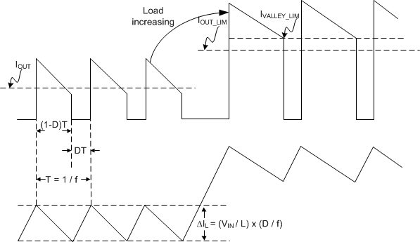
TPS61230A CL_SLVSCZ5.gifFigure 13. Current Limit Operation