ZHCSGE4B December 2010 – March 2017 TPS61240-Q1
PRODUCTION DATA.
6 Specifications
6.1 Absolute Maximum Ratings
over operating free-air temperature range (unless otherwise noted)(1)(2)| MIN | MAX | UNIT | ||
|---|---|---|---|---|
| Input voltage, VI (on VIN, L, and EN) | –0.3 | 7 | V | |
| Voltage on VOUT | –2 | 7 | V | |
| Voltage on FB | –2 | 14 | V | |
| Peak output current | Internally limited | |||
| Operating junction temperature, TJ | –40 | 125 | °C | |
| Storage temperature, Tstg | –65 | 150 | °C | |
(1) Stresses beyond those listed under Absolute Maximum Ratings may cause permanent damage to the device. These are stress ratings only, which do not imply functional operation of the device at these or any other conditions beyond those indicated under Recommended Operating Conditions. Exposure to absolute-maximum-rated conditions for extended periods may affect device reliability.
6.2 ESD Ratings
| VALUE | UNIT | |||
|---|---|---|---|---|
| V(ESD) | Electrostatic discharge | Human-body model (HBM), per AEC Q100-002(1) | ±2000 | V |
| Charged-device model (CDM), per AEC Q100-011 | ±1000 | |||
(1) AEC Q100-002 indicates that HBM stressing shall be in accordance with the ANSI/ESDA/JEDEC JS-001 specification.
6.3 Recommended Operating Conditions
over operating free-air temperature range (unless otherwise noted)| MIN | NOM | MAX | UNIT | |||
|---|---|---|---|---|---|---|
| Supply voltage at VIN | 2.3 | 5.5 | V | |||
| L | Inductance | 1 | 2.2 | µH | ||
| Cout | Output capacitance | 1 | 20 | µF | ||
| TA | Operating ambient temperature(1) | TPS61240IDRVRQ1 | –40 | 85 | °C | |
| TPS61240TDRVRQ1 | –40 | 105 | °C | |||
(1) In applications where high power dissipation, poor package thermal resistance, or both are present, the maximum ambient temperature may have to be derated. Maximum ambient temperature (TA(max)) is dependent on the maximum operating junction temperature (TJ(max)), the maximum power dissipation of the device in the application (PD(max)), and the junction-to-ambient thermal resistance of the device or package in the application (RθJA), as given by the following equation: TA(max)= TJ(max) – (RθJA × PD(max))
6.4 Thermal Information
| THERMAL METRIC(1) | TPS61240-Q1 | UNIT | |
|---|---|---|---|
| DRV (WSON) | |||
| 6 PINS | |||
| RθJA | Junction-to-ambient thermal resistance | 67.8 | °C/W |
| RθJC(top) | Junction-to-case (top) thermal resistance | 71.4 | °C/W |
| RθJB | Junction-to-board thermal resistance | 37.5 | °C/W |
| ψJT | Junction-to-top characterization parameter | 1.8 | °C/W |
| ψJB | Junction-to-board characterization parameter | 37.8 | °C/W |
| RθJC(bot) | Junction-to-case (bottom) thermal resistance | 8.7 | °C/W |
(1) For more information about traditional and new thermal metrics, see the Semiconductor and IC Package Thermal Metrics application report.
6.5 Electrical Characteristics
Over full operating ambient temperature range with typical values at TA = 25°C. Specifications apply for condition VIN = EN = 3.6 V (unless otherwise noted). External components CIN = 2.2 μF, COUT = 4.7 μF (0603), and L = 1μH (refer to Typical Applications section).| PARAMETER | TEST CONDITIONS | MIN | TYP | MAX | UNIT | |
|---|---|---|---|---|---|---|
| DC/DC STAGE | ||||||
| VIN | Input voltage range | 2.3 | 5.5 | V | ||
| VOUT | Fixed output voltage range | 2.3 V ≤ VIN ≤ VOUT, 0 mA ≤ IOUT ≤ 200 mA | 4.9 | 5 | 5.1 | V |
| VO_Ripple | Ripple voltage, PWM mode | ILOAD = 150 mA | 20 | mVpp | ||
| Output current | VIN = 2.3 V to 5.5 V | 200 | mA | |||
| ISW | Switch valley current limit | VOUT = VGS = 5 V | 500 | 600 | mA | |
| Short circuit current | VOUT = VGS = 5 V | 200 | 350 | mApk | ||
| High side MOSFET on-resistance(1) |
VIN = VGS = 5 V, TA = 25°C(1) | 290 | mΩ | |||
| Low Side MOSFET on-resistance(1) |
VIN = VGS = 5 V, TA = 25°C(1) | 250 | mΩ | |||
| Operating quiescent current | IOUT = 0 mA, power save mode, device not switching | 30 | 40 | μA | ||
| Shutdown current | TPS61240IDRVRQ1, EN = GND | 1.5 | μA | |||
| TPS61240TDRVRQ1, EN = GND | 2.5 | |||||
| Reverse leakage current VOUT | EN = 0 V, VOUT = 5 V | 2.5 | μA | |||
| Leakage current from battery to VOUT |
EN = GND | 2.5 | μA | |||
| Line transient response | VIN = 600 mVp-p AC square wave, 200 Hz, 12.5% DC at 50 mA or 200 mA load |
±25 | ±50 | mVpk | ||
| Load transient response | 0 mA to 50 mA, 50 mA to 0 mA, VIN = 3.6 V, TRise = TFall = 0.1 μs |
50 | mVpk | |||
| 50 mA to 200 mA, 200 mA to 50 mA, VIN = 3.6 V, TRise = TFall = 0.1 μs |
150 | |||||
| IIN | Input bias current, EN | EN = GND or VIN | 0.01 | 1.0 | μA | |
| VUVLO | Undervoltage lockout threshold | Falling | 2.0 | 2.1 | V | |
| Rising | 2.1 | 2.2 | V | |||
| CONTROL STAGE | ||||||
| VIH | High level input voltage, EN | 2.3 V ≤ VIN ≤ 5.5 V | 1.0 | V | ||
| VIL | Low level input voltage, EN | 2.3 V ≤ VIN ≤ 5.5 V | 0.4 | V | ||
| OVC | Input over-voltage threshold | Falling | 5.9 | V | ||
| Rising | 6 | |||||
| tStart | Start-up time | Time from active EN to start switching, no-load until VOUT is stable 5 V | 300 | μs | ||
| DC/DC STAGE | ||||||
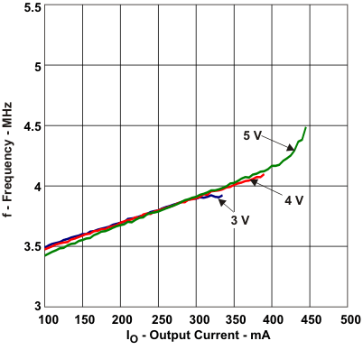
| Freq | See Figure 7 | 3.5 | MHz | |||
| TSD | Thermal shutdown | Increasing junction temperature | 140 | °C | ||
| Thermal shutdown hysteresis | Decreasing junction temperature | 20 | °C | |||
(1) DRV package has an increased RDSon of about 40 mΩ due to bond wire resistance.
6.6 Typical Characteristics
Table 1. Table of Graphs
| Figure | ||
|---|---|---|
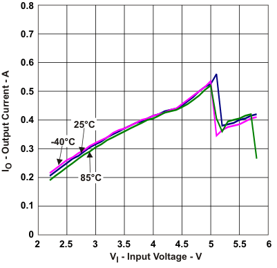
| Maximum output current | vs Input voltage | Figure 1 |
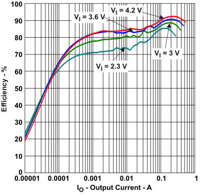
| Efficiency | vs Output current, VOUT = 5 V, VIN = [2.3 V, 3 V, 3.6 V, 4.2 V] | Figure 2 |
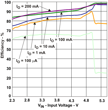
| vs Input voltage, VOUT = 5 V, IOUT = [100 µA, 1 mA, 10 mA, 100 mA, 200 mA] | Figure 3 | |
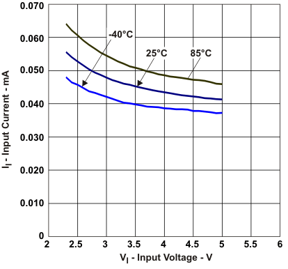
| Input current | at No output load (PFM Mode) | Figure 4 |
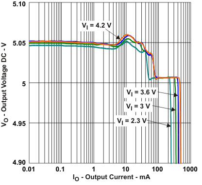
| Output voltage | vs Output current, VOUT = 5 V, VIN = [2.3 V, 3 V, 3.6 V, 4.2 V] | Figure 5 |
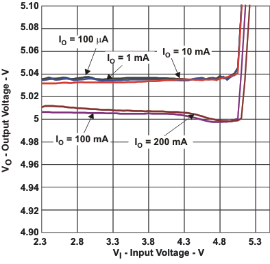
| vs Input voltage | Figure 6 | |
| Frequency | vs Output load, VOUT = 5 V, VIN = [3 V, 4 V, 5 V] | Figure 7 |
