SLVS806D April 2009 – December 2015 TPS61240 , TPS61241
PRODUCTION DATA.
- 1 Features
- 2 Applications
- 3 Description
- 4 Revision History
- 5 Device Options
- 6 Pin Configuration and Functions
- 7 Specifications
- 8 Parameter Measurement Information
- 9 Detailed Description
- 10Application and Implementation
- 11Power Supply Recommendations
- 12Layout
- 13Device and Documentation Support
- 14Mechanical, Packaging, and Orderable Information
封装选项
机械数据 (封装 | 引脚)
散热焊盘机械数据 (封装 | 引脚)
- DRV|6
订购信息
9 Detailed Description
9.1 Overview
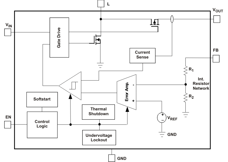
The TPS6124x device is a highly efficient synchronous step-up DC-DC converter optimized for products powered by either a three-cell alkaline, NiCd or NiMH, or one-cell Li-Ion or Li-Polymer battery. The TPS6124x supports output currents up to 450 mA. The TPS61240 has an input valley current limit of 500 mA, and the TPS61241 has an input valley current of 600 mA. The TPS6124x boost converter is based on a quasi-constant on-time valley current mode control scheme. TPS6124x allows the use of small inductors and capacitors to achieve a small solution size. During shutdown, the load is completely disconnected from the battery.
9.2 Functional Block Diagram

9.3 Feature Description
9.3.1 Operation
The TPS6124x boost converter operates with typically 3.5-MHz fixed frequency pulse width modulation (PWM) at moderate to heavy load currents. At light load currents the converter will automatically enter power save mode and operates then in PFM (Pulse Frequency Modulation) mode. During PWM operation the converter uses a unique fast response quasi-constant on-time valley current mode controller scheme which allows “Best in Class” line and load regulation allowing the use of small ceramic input and output capacitors.
Based on the VIN/VOUT ratio, a simple circuit predicts the required on-time. At the beginning of the switching cycle, the low-side N-MOS switch is turned-on and the inductor current ramps up to a defined peak current. In the second phase, once the peak current is reached, the current comparator trips, the on-timer is reset turning off the switch, and the current through the inductor then decays to an internally set valley current limit. Once this occurs, the on-timer is set to turn the boost switch back on again and the cycle is repeated.
9.3.2 Current Limit Operation
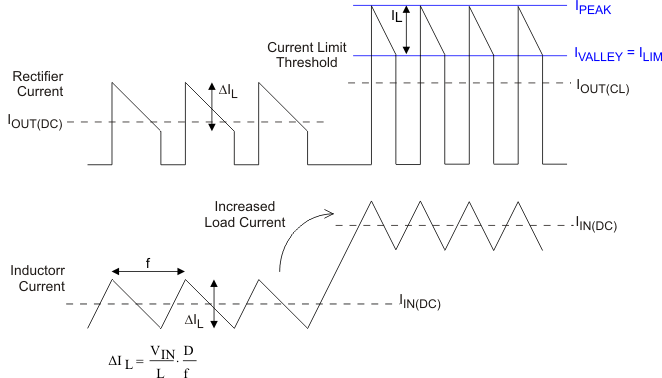
The current limit circuit employs a valley current sensing scheme. Current limit detection occurs during the off time through sensing of the voltage drop across the synchronous rectifier.
The output voltage is reduced as the power stage of the device operates in a constant current mode. The maximum continuous output current (IOUT(CL)), before entering current limit operation, can be defined by Equation 1 as shown.

Figure 9 illustrates the inductor and rectifier current waveforms during current limit operation. The output current, IOUT, is the average of the rectifier ripple current waveform. When the load current is increased such that the lower peak is above the current limit threshold, the off time is lengthened to allow the current to decrease to this threshold before the next on-time begins (so called frequency fold-back mechanism).
 Figure 9. Inductor/Rectifier Currents in Current Limit Operation
9.3.3 Undervoltage Lockout
The undervoltage lockout circuit prevents the device from malfunctioning at low input voltages and from excessive discharge of the battery. It disables the output stage of the converter once the falling VIN trips the undervoltage lockout threshold VUVLO. The undervoltage lockout threshold VUVLO for falling VIN is typically 2.0 V. The device starts operation once the rising VIN trips undervoltage lockout threshold VUVLO again at typically 2.1 V.
9.3.4 Input Overvoltage Protection
In the event of an overvoltage condition appearing on the input rail, the output voltage will also experience the overvoltage due to being in dropout condition. A input overvoltage protection feature has been implemented into the TPS6124x which has an input overvoltage threshold of 6.0 V. Once this level is triggered, the device will go into a shutdown mode to protect itself. If the voltage drops to 5.9 V or below, the device will startup once more into normal operation.
9.3.5 Enable
The device is enabled setting EN pin to high. At first, the internal reference is activated and the internal analog circuits are settled. Afterwards, the soft start is activated and the output voltage is ramped up. The output voltages reaches its nominal value in typically 250 μs after the device has been enabled.
The EN input can be used to control power sequencing in a system with various DC-DC converters. The EN pin can be connected to the output of another converter, to drive the EN pin high and getting a sequencing of supply rails. With EN = GND, the device enters shutdown mode.
9.3.6 Soft Start
The TPS6124x has an internal soft start circuit that controls the ramp up of the output voltage. The output voltages reaches its nominal value within tStart of typically 250μs after EN pin has been pulled to high level. The output voltage ramps up from 5% to its nominal value within tRAMP of typically 300 μs.
This limits the inrush current in the converter during start up and prevents possible input voltage drops when a battery or high impedance power source is used.
During soft start, the switch current limit is reduced to 300 mA until the output voltage reaches VIN. Once the output voltage trips this threshold, the device operates with its nominal current limit ILIMT.
9.3.7 Load Disconnect
Load disconnect electrically removes the output from the input of the power supply when the supply is disabled. This is especially important during shutdown. In shutdown of a boost converter, the load is still connected to the input through the inductor and catch diode. Since the input voltage is still connected to the output, a small current continues to flow, even when the supply is disabled. Even small leakage currents significantly reduce battery life during extended periods of off time.
The benefit of this implemented feature for the system design engineer is that the battery is not depleted during shutdown of the converter. No additional components must be added to the design to make sure that the battery is disconnected from the output of the converter.
9.3.8 Thermal Shutdown
As soon as the junction temperature, TJ, exceeds 140°C (typical) the device goes into thermal shutdown. In this mode, the High Side and Low Side MOSFETs are turned-off. When the junction temperature falls below the thermal shutdown hysteresis, the device continuous operation.
9.4 Device Functional Modes
9.4.1 Power Save Mode
The TPS6124x family of devices integrates a power save mode to improve efficiency at light load. In power save mode the converter only operates when the output voltage trips below a set threshold voltage. It ramps up the output voltage with several pulses and goes into power save mode once the output voltage exceeds the set threshold voltage.

The PFM mode is left and PWM mode entered in case the output current can not longer be supported in PFM mode.