SLVS806D April   2009  – December 2015 TPS61240 , TPS61241

PRODUCTION DATA.  

  1. Features
  2. Applications
  3. Description
  4. Revision History
  5. Device Options
  6. Pin Configuration and Functions
  7. Specifications
    1. 7.1 Absolute Maximum Ratings
    2. 7.2 ESD Ratings
    3. 7.3 Recommended Operating Conditions
    4. 7.4 Thermal Information
    5. 7.5 Electrical Characteristics
    6. 7.6 Typical Characteristics
      1. 7.6.1 Table of Graphs
  8. Parameter Measurement Information
  9. Detailed Description
    1. 9.1 Overview
    2. 9.2 Functional Block Diagram
    3. 9.3 Feature Description
      1. 9.3.1 Operation
      2. 9.3.2 Current Limit Operation
      3. 9.3.3 Undervoltage Lockout
      4. 9.3.4 Input Overvoltage Protection
      5. 9.3.5 Enable
      6. 9.3.6 Soft Start
      7. 9.3.7 Load Disconnect
      8. 9.3.8 Thermal Shutdown
    4. 9.4 Device Functional Modes
      1. 9.4.1 Power Save Mode
  10. 10Application and Implementation
    1. 10.1 Application Information
    2. 10.2 Typical Application
      1. 10.2.1 Design Requirements
      2. 10.2.2 Detailed Design Procedure
        1. 10.2.2.1 Programming the Output Voltage
        2. 10.2.2.2 Inductor Selection
        3. 10.2.2.3 Input Capacitor
        4. 10.2.2.4 Output Capacitor
        5. 10.2.2.5 Checking Loop Stability
      3. 10.2.3 Application Curves
    3. 10.3 System Examples
  11. 11Power Supply Recommendations
  12. 12Layout
    1. 12.1 Layout Guidelines
    2. 12.2 Layout Example
    3. 12.3 Thermal Considerations
  13. 13Device and Documentation Support
    1. 13.1 Device Support
      1. 13.1.1 Third-Party Products Disclaimer
    2. 13.2 Related Links
    3. 13.3 Trademarks
    4. 13.4 Electrostatic Discharge Caution
    5. 13.5 Glossary
  14. 14Mechanical, Packaging, and Orderable Information
    1. 14.1 Chip Scale Package Dimensions

封装选项

机械数据 (封装 | 引脚)
散热焊盘机械数据 (封装 | 引脚)
订购信息

14 Mechanical, Packaging, and Orderable Information

The following pages include mechanical, packaging, and orderable information. This information is the most current data available for the designated devices. This data is subject to change without notice and revision of this document. For browser-based versions of this data sheet, refer to the left-hand navigation.
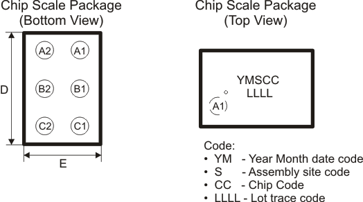
14.1 Chip Scale Package Dimensions

The TPS6124x device is available in a 6-bump chip scale package (YFF, NanoFree™). The package dimensions are given as:

D E
Max = 1280 µm Max = 890 µm
Min = 1220 µm Min = 830 µm
TPS61240 TPS61241 wcspkg_lvs806.gif