ZHCSCS7A September   2014  – September 2014 TPS61291

PRODUCTION DATA.  

  1. 特性
  2. 应用
  3. 说明
  4. 修订历史记录
  5. Pin Configuration and Functions
  6. Specifications
    1. 6.1 Absolute Maximum Ratings
    2. 6.2 Handling Ratings
    3. 6.3 Recommended Operating Conditions
    4. 6.4 Thermal Information
    5. 6.5 Electrical Characteristics
    6. 6.6 Typical Characteristics
  7. Detailed Description
    1. 7.1 Overview
    2. 7.2 Functional Block Diagram
    3. 7.3 Feature Description
      1. 7.3.1 Bypass / Boost Mode Operation EN/BYP
      2. 7.3.2 Output Voltage Selection VSEL
      3. 7.3.3 Feedback Divider Disconnect
      4. 7.3.4 Undervoltage Lockout
      5. 7.3.5 Overtemperature Protection
      6. 7.3.6 Overvoltage Protection
    4. 7.4 Device Functional Modes
      1. 7.4.1 Boost Mode Operation
      2. 7.4.2 Bypass Mode Operation
      3. 7.4.3 Controlled Transition into Bypass Mode
      4. 7.4.4 Operation at Output Overload
      5. 7.4.5 Startup
  8. Applications and Implementation
    1. 8.1 Application Information
    2. 8.2 Typical Application
      1. 8.2.1 Design Requirements
      2. 8.2.2 Detailed Design Procedure
        1. 8.2.2.1 Inductor Selection
        2. 8.2.2.2 Input and Output Capacitor Selection
      3. 8.2.3 Application Curves
  9. Power Supply Recommendations
  10. 10Layout
    1. 10.1 Layout Guidelines
    2. 10.2 Layout Example
  11. 11器件和文档支持
    1. 11.1 器件支持
      1. 11.1.1 第三方米6体育平台手机版_好二三四免责声明
    2. 11.2 文档支持
      1. 11.2.1 相关文档 
    3. 11.3 商标
    4. 11.4 静电放电警告
    5. 11.5 术语表
  12. 12机械封装和可订购信息

封装选项

机械数据 (封装 | 引脚)
散热焊盘机械数据 (封装 | 引脚)
订购信息

8 Applications and Implementation

NOTE

Information in the following applications sections is not part of the TI component specification, and TI does not warrant its accuracy or completeness. TI’s customers are responsible for determining suitability of components for their purposes. Customers should validate and test their design implementation to confirm system functionality.

8.1 Application Information

The TPS61291 is a boost converter with pin selectable output voltages and an integrated bypass mode. In bypass operation, the device provides a direct path from the input to the system and allows a low power micro controller (MCU) to operate directly from a single 3V Li-MnO2 battery or dual alkaline battery cells. In bypass mode, the quiescent current consumption is typically only 15nA and supports low power modes of MCUs such as the MSP430. In boost mode operation, the device provides a regulated output voltage (e.g. 3.3V) to supply circuits which require a higher voltage than provided by the battery. See Figure 8.

The device also extends battery life in applications which can run partially directly from the battery, but need a boost conversion to maintain sufficient system voltage when the battery voltage drops due to discharge. In this case, the system runs off the battery in bypass mode operation until the battery voltage trips the minimum system operating voltage. Then the system turns on the boost converter, providing a sufficient output voltage down to the cut off voltage of the battery. See Figure 9 and Figure 26.

8.2 Typical Application

TPS61291_app_frontpage.gifFigure 8. Typical Application Circuit with Regulated 3.3V VOUT / VBAT
TPS61291_app_bat_Ext.gifFigure 9. Bypass Mode / Boost Mode Operation to Maintain Sufficient System Voltage

8.2.1 Design Requirements

The TPS61291 is a highly integrated boost converter. The output voltage is set internally via a VSEL pin without any additional components. For operation, only an input capacitor, output capacitor, and an inductor are required. Table 1 shows the components used for the application characteristic curves.

Table 1. Components for Application Characteristic Curves(1)

Reference Description Value Manufacturer
TPS61291 Low Iq Boost Converter with Bypass Operation Texas Instruments
CIN Input capacitor 10µF Murata GRM219R61A106KE44D
COUT Output capacitor 22µF Murata GRM21BR60J226ME39L
L Inductor 3.3µH Coilcraft LPS3314 3R3
(1) See the Third-Party Products Disclaimer in the Device Support section.

8.2.2 Detailed Design Procedure

The external components have to fulfill the needs of the application but also the stability criteria of the device's control loop. The TPS61291 is optimized to work within a range of L and C combinations. The LC output filter inductance and capacitance must be considered together. The output capacitor sets the corner frequency of the converter while the inductor creates a Right-Half-Plane-Zero degrading the stability of the converter. Consequently with a larger inductor a bigger capacitor has to be used to guarantee a stable loop. Table 2 shows the output filter component selection.

Table 2. Recommended LC Output Filter Combinations

Output voltage [V] Inductor value [µH](2) Output capacitor value [µF](1)
22 22 + 10 2 x 22
3.3 / 3.0 3.3 (3)
4.7
2.5 2.2
3.3 (3)
(1) Capacitance tolerance and bias voltage de-rating is anticipated. The effective capacitance can vary by 20% and -50%.
(2) Inductor tolerance and current de-rating is anticipated. The effective inductance can vary by 20% and -30%.
(3) This LC combination is the standard value and recommended for most applications.

8.2.2.1 Inductor Selection

The device is optimized to operate with a 3.3µH inductor value. Other inductor values can be used, per Table 2. The maximum inductor current can be approximated by the ILMAX, from Equation 1. For proper operation, the inductor needs to be rated for a saturation current which is higher than the switch current limit of typically 1A. Table 3 lists inductors that have been tested with the TPS61291.

Equation 1. q_ILMAX_TPS61291_300mA_ripple.gif

Table 3. List of Inductors(1)

INDUCTANCE DIMENSIONS [mm3] TYPE SUPPLIER
3.3 3.3 x 3.3 x 1.3 LPS3314 Coilcraft
3.3 2.95 x 2.95 x 1.4 LPS3015
3.3 3 x 2.5 x 1.5 VLF302515 TDK
3.3 2 x 2 x 1.2 MDMK2020T3R3M Taiyo Yuden
3.3 2.5 x 2.0 x 1.2 DFE252012 Toko
3.3 3.0 x 3.0 x 1.5 74438335033 Würth
(1) See the Third-Party Products Disclaimer in the Device Support section.

8.2.2.2 Input and Output Capacitor Selection

For best output and input voltage filtering, low ESR X5R or X7R ceramic capacitors are recommended. The input capacitor minimizes input voltage ripple, suppresses input voltage spikes and provides a stable system rail for the device. At least a 10μF or larger input capacitor is recommended for operation. In applications in which the power source (e.g. certain battery chemistries) shows an internal resistance characteristic, a larger input capacitor might be used to buffer the supply voltage for the TPS61291. The recommended typical output capacitor value is 22 μF and can vary as outlined in the output filter selection Table 2.

8.2.3 Application Curves

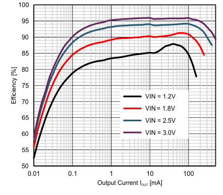
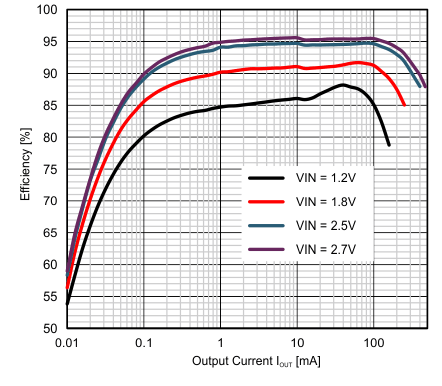
eff_vs_IOUT_VO_3_3V.gif
EN/BYP = high L = 3.3µH VSEL = GND
Figure 10. Efficiency vs IOUT, VOUT = 3.3V
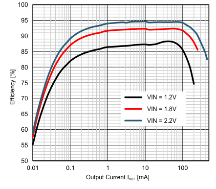
eff_vs_IOUT_VO_2p5V.gif
EN/BYP = high L = 3.3µH VSEL = open
Figure 12. Efficiency vs IOUT, VOUT = 2.5V
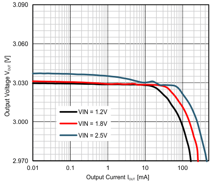
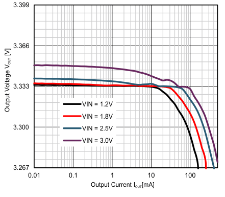
app_tG_VO_vsIO_3p0V_VO.gif
EN/BYP = high L = 3.3µH VSEL = VOUT
Figure 14. Output Voltage vs Output Current VOUT = 3.0V
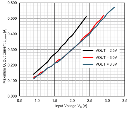
app_TG_IO_MAX_25DGC_1pcdrop.gif
EN/BYP = high ISW = 1000mA (typical)
L = 3.3µH Boost mode operation
Figure 16. Maximum Output Current
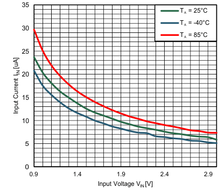
IIN_no_load_VO_3_0V.gif
VOUT = 3.0 V L = 3.3 µH COUT = 22 µF
IOUT = 0 mA Device switching
Figure 18. Supply Current vs. VIN, VOUT = 3.0V, IOUT = 0mA
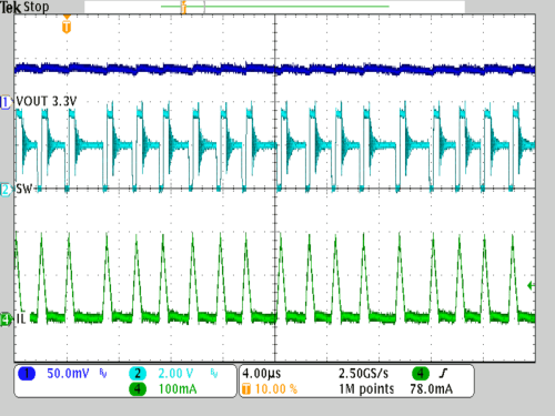
SP_PFM_200R_load_VO_3_3V_VIN_2V.gif
VIN = 2.0 V L = 3.3 µH COUT = 22 µF
VOUT = 3.3 V IOUT = 15mA VSEL = GND
EN/BYP = high
Figure 20. Discontinuous Conduction Mode Operation,
VOUT = 3.3V
SP_Loadtransient_20mA_150mA_VO_3_3V_VIN_1_8V_3_3uH_CO22uF.gif
VIN = 1.8V L = 3.3µH COUT = 22 µF
VOUT = 3.3V VSEL = GND
ILOAD 20mA /150mA
Figure 22. Load Transient Response
SP_Line_transient_VIN3V_2p5V_VO_3_3V_100R_3_3uH_CO22uF.gif
VIN = 2.5V/3V L = 3.3µH COUT = 22 µF
VOUT = 3.3V VSEL = GND Load =100Ω
Figure 24. Line Transient Response
SP_boost_bypass_mode_VIN_sweep_VO_3_3V_3_3uH_CO22uF_5mA.gif
VIN = 0.9V to 3V VSEL = Open ILOAD = 5mA
VOUT = 2.5V EN/BYP externally controlled
Bypass / Boost mode operation
Figure 26. Bypass / Boost Mode Operation
eff_vs_IOUT_VO_3_0V.gif
EN/BYP = high L = 3.3µH VSEL = VOUT
Figure 11. Efficiency vs IOUT, VOUT = 3.0V
app_tG_VO_vsIO_3p3V_VO.gif
EN/BYP = high L = 3.3µH VSEL = GND
Figure 13. Output Voltage vs Output Current VOUT = 3.3V
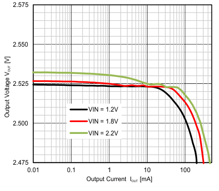
app_tG_VO_vsIO_2p5V_VO.gif
EN/BYP = high L = 3.3µH VSEL = open
Figure 15. Output Voltage vs Output Current VOUT = 2.5V
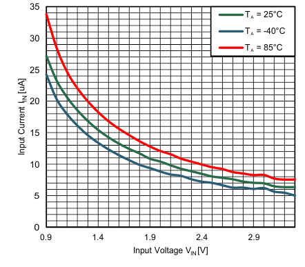
IIN_no_load_VO_3_3V.gif
VOUT = 3.3 V L = 3.3 µH COUT = 22 µF
IOUT = 0 mA Device switching
Figure 17. Supply Current vs. VIN, VOUT = 3.3V, IOUT = 0mA
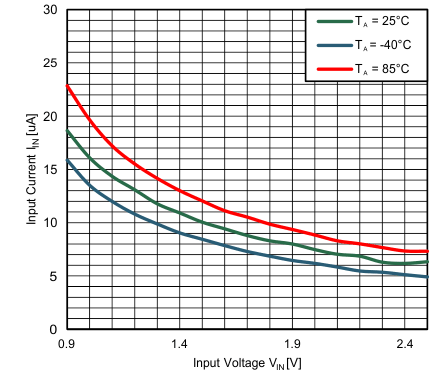
IIN_no_load_VO_2_5V.gif
VOUT = 2.5 V L = 3.3 µH COUT = 22 µF
IOUT = 0 mA Device switching
Figure 19. Supply Current vs. VIN, VOUT = 2.5V, IOUT = 0mA
SP_VO_3_3V_IOUT_150mA_VIN_1_8V_3_3uH_CO22uF.gif
VIN = 1.8 V L = 3.3 µH COUT = 22 µF
VOUT = 3.3 V IOUT = 150 mA
VSEL = GND EN/BYP = high
Figure 21. Continuous Conduction Mode Operation,
VOUT = 3.3V
SP_AC_load_sweep_1mA_200mA_VIN_1p8V_VO_3_3V_3_3uH_CO22uF.gif
VIN = 1.8V L = 3.3µH COUT = 22 µF
VOUT = 3.3V VSEL = GND
ILOAD 1mA/200mA
Figure 23. AC Load Sweep
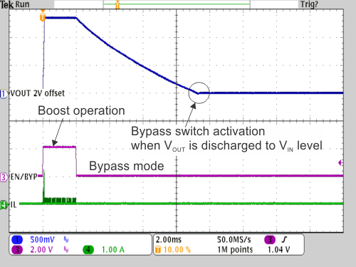
SP_boost_mode_bypass_mode_transition_VO_3_3V_1l_load.gif
VIN = 2.0V L = 3.3µH COUT = 22 µF
VOUT = 3.3V VSEL = GND RLOAD = 1kΩ
Figure 25. Boost Mode / Bypass Mode Transition
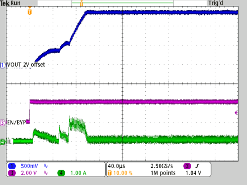
SP_startup_100R_load_VO_3_3V_VIN_2V.gif
VIN = 2.0V L = 3.3µH COUT = 22 µF
VOUT = 3.3V VSEL = GND RLOAD = 100Ω
Figure 27. Startup in Boost Mode